SNOSD10F April   2016  – May 2020 LMG3410R070 , LMG3411R070

PRODUCTION DATA.  

  1. Features
  2. Applications
  3. Description
    1.     Device Images
      1.      Simplified Block Diagram
      2.      Switching Performance at >100 V/ns
  4. Revision History
  5. Pin Configuration and Functions
    1.     Pin Functions
  6. Specifications
    1. 6.1 Absolute Maximum Ratings
    2. 6.2 ESD Ratings
    3. 6.3 Recommended Operating Conditions
    4. 6.4 Thermal Information
    5. 6.5 Electrical Characteristics
    6. 6.6 Switching Characteristics
    7. 6.7 Typical Characteristics
  7. Parameter Measurement Information
    1. 7.1 Switching Parameters
      1. 7.1.1 Turn-on Delays
      2. 7.1.2 Turn-off Delays
      3. 7.1.3 Drain Slew Rate
      4. 7.1.4 Turn-on and Turn-off Energy
  8. Detailed Description
    1. 8.1 Overview
    2. 8.2 Functional Block Diagram
    3. 8.3 Feature Description
      1. 8.3.1 Direct-Drive GaN Architecture
      2. 8.3.2 Internal Buck-Boost DC-DC Converter
      3. 8.3.3 Internal Auxiliary LDO
      4. 8.3.4 Fault Detection
        1. 8.3.4.1 Over-current Protection
        2. 8.3.4.2 Over-Temperature Protection and UVLO
      5. 8.3.5 Drive Strength Adjustment
    4. 8.4 Device Functional Modes
      1. 8.4.1 Low-Power Mode
  9. Application and Implementation
    1. 9.1 Application Information
    2. 9.2 Typical Application
      1. 9.2.1 Design Requirements
      2. 9.2.2 Detailed Design Procedure
        1. 9.2.2.1 Slew Rate Selection
          1. 9.2.2.1.1 Startup and Slew Rate with Bootstrap High-Side Supply
        2. 9.2.2.2 Signal Level-Shifting
        3. 9.2.2.3 Buck-Boost Converter Design
      3. 9.2.3 Application Curves
    3. 9.3 Paralleling GaN Devices
    4. 9.4 Do's and Don'ts
  10. 10Power Supply Recommendations
    1. 10.1 Using an Isolated Power Supply
    2. 10.2 Using a Bootstrap Diode
      1. 10.2.1 Diode Selection
      2. 10.2.2 Managing the Bootstrap Voltage
      3. 10.2.3 Reliable Bootstrap Start-up
  11. 11Layout
    1. 11.1 Layout Guidelines
      1. 11.1.1 Power Loop Inductance
      2. 11.1.2 Signal Ground Connection
      3. 11.1.3 Bypass Capacitors
      4. 11.1.4 Switch-Node Capacitance
      5. 11.1.5 Signal Integrity
      6. 11.1.6 High-Voltage Spacing
      7. 11.1.7 Thermal Recommendations
    2. 11.2 Layout Example
  12. 12Device and Documentation Support
    1. 12.1 Device Support
      1. 12.1.1 Third-Party Products Disclaimer
    2. 12.2 Documentation Support
      1. 12.2.1 Related Documentation
    3. 12.3 Receiving Notification of Documentation Updates
    4. 12.4 Community Resources
    5. 12.5 Trademarks
    6. 12.6 Electrostatic Discharge Caution
    7. 12.7 Glossary
  13. 13Mechanical, Packaging, and Orderable Information

Package Options

Mechanical Data (Package|Pins)
Thermal pad, mechanical data (Package|Pins)
Orderable Information

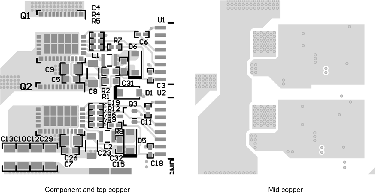
Layout Example

Correct layout of the LMG341xR070 and its surrounding components is essential for correct operation. The layout shown here reflects the power stage schematic in Figure 14. It may be possible to obtain acceptable performance with alternate layout schemes, however this layout has been shown to produce good results and is intended as a guideline.
LMG3410R070 LMG3411R070 ex_layout_snosd10.pngFigure 19. Example Half-Bridge Layout