SNOSDA7F September   2020  – August 2024 LMG3422R030 , LMG3426R030 , LMG3427R030

PRODUCTION DATA  

  1.   1
  2. Features
  3. Applications
  4. Description
  5. Pin Configuration and Functions
  6. Specifications
    1. 5.1 Absolute Maximum Ratings
    2. 5.2 ESD Ratings
    3. 5.3 Recommended Operating Conditions
    4. 5.4 Thermal Information
    5. 5.5 Electrical Characteristics
    6. 5.6 Switching Characteristics
    7. 5.7 Typical Characteristics
  7. Parameter Measurement Information
    1. 6.1 Switching Parameters
      1. 6.1.1 Turn-On Times
      2. 6.1.2 Turn-Off Times
      3. 6.1.3 Drain-Source Turn-On Slew Rate
      4. 6.1.4 Turn-On and Turn-Off Switching Energy
      5. 6.1.5 Zero-Voltage Detection Times (LMG3426R030 only)
      6. 6.1.6 Zero-Current Detection Times (LMG3427R030 only)
    2. 6.2 Safe Operation Area (SOA)
      1. 6.2.1 Repetitive SOA
  8. Detailed Description
    1. 7.1 Overview
    2. 7.2 Functional Block Diagram
      1. 7.2.1 LMG3422R030 Functional Block Diagram
      2. 7.2.2 LMG3426R030 Functional Block Diagram
      3. 7.2.3 LMG3427R030 Functional Block Diagram
    3. 7.3 Feature Description
      1. 7.3.1  GaN FET Operation Definitions
      2. 7.3.2  Direct-Drive GaN Architecture
      3. 7.3.3  Drain-Source Voltage Capability
      4. 7.3.4  Internal Buck-Boost DC-DC Converter
      5. 7.3.5  VDD Bias Supply
      6. 7.3.6  Auxiliary LDO
      7. 7.3.7  Fault Protection
        1. 7.3.7.1 Overcurrent Protection and Short-Circuit Protection
        2. 7.3.7.2 Overtemperature Shutdown Protection
        3. 7.3.7.3 UVLO Protection
        4. 7.3.7.4 High-Impedance RDRV Pin Protection
        5. 7.3.7.5 Fault Reporting
      8. 7.3.8  Drive-Strength Adjustment
      9. 7.3.9  Temperature-Sensing Output
      10. 7.3.10 Ideal-Diode Mode Operation
        1. 7.3.10.1 Overtemperature-Shutdown Ideal-Diode Mode
      11. 7.3.11 Zero-Voltage Detection (ZVD) (LMG3426R030 only)
      12. 7.3.12 Zero-Current Detection (ZCD) (LMG3427R030 only)
    4. 7.4 Start-Up Sequence
    5. 7.5 Device Functional Modes
  9. Application and Implementation
    1. 8.1 Application Information
    2. 8.2 Typical Application
      1. 8.2.1 Design Requirements
      2. 8.2.2 Detailed Design Procedure
        1. 8.2.2.1 Slew Rate Selection
        2. 8.2.2.2 Signal Level-Shifting
        3. 8.2.2.3 Buck-Boost Converter Design
      3. 8.2.3 Application Curves
    3. 8.3 Do's and Don'ts
    4. 8.4 Power Supply Recommendations
      1. 8.4.1 Using an Isolated Power Supply
      2. 8.4.2 Using a Bootstrap Diode
        1. 8.4.2.1 Diode Selection
        2. 8.4.2.2 Managing the Bootstrap Voltage
    5. 8.5 Layout
      1. 8.5.1 Layout Guidelines
        1. 8.5.1.1 Solder-Joint Reliability
        2. 8.5.1.2 Power-Loop Inductance
        3. 8.5.1.3 Signal-Ground Connection
        4. 8.5.1.4 Bypass Capacitors
        5. 8.5.1.5 Switch-Node Capacitance
        6. 8.5.1.6 Signal Integrity
        7. 8.5.1.7 High-Voltage Spacing
        8. 8.5.1.8 Thermal Recommendations
      2. 8.5.2 Layout Examples
  10. Device and Documentation Support
    1. 9.1 Documentation Support
      1. 9.1.1 Related Documentation
    2. 9.2 Receiving Notification of Documentation Updates
    3. 9.3 Support Resources
    4. 9.4 Trademarks
    5. 9.5 Electrostatic Discharge Caution
    6. 9.6 Export Control Notice
    7. 9.7 Glossary
  11. 10Revision History
  12. 11Mechanical, Packaging, and Orderable Information

Package Options

Refer to the PDF data sheet for device specific package drawings

Mechanical Data (Package|Pins)
  • RQZ|54
Thermal pad, mechanical data (Package|Pins)
Orderable Information

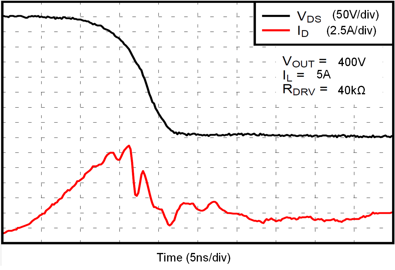
Application Curves

LMG3422R030 LMG3426R030 LMG3427R030 Turn-On Waveform in
                        Application ExampleFigure 8-5 Turn-On Waveform in Application Example
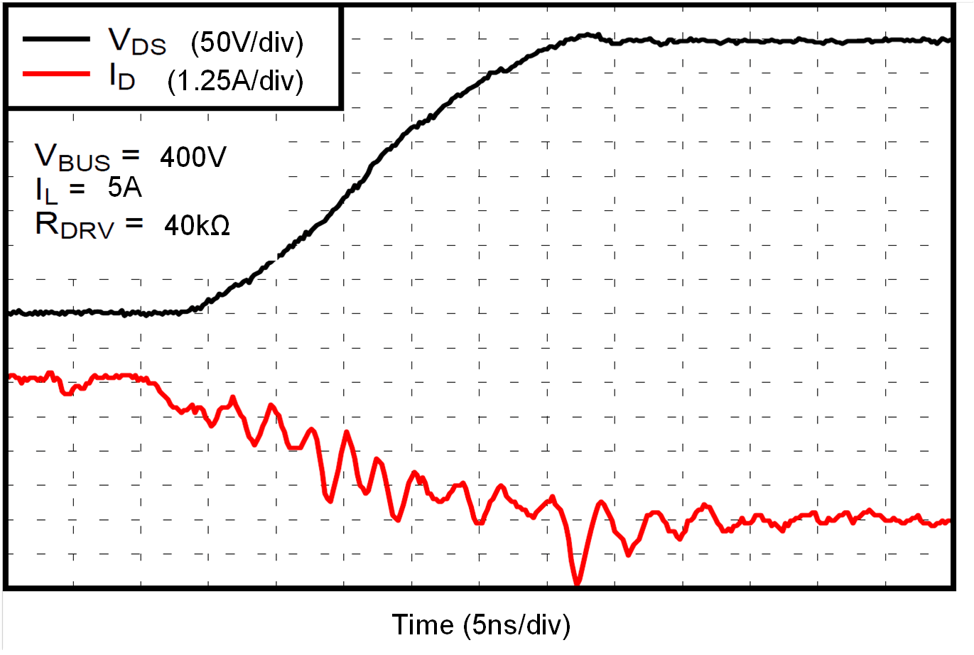
LMG3422R030 LMG3426R030 LMG3427R030 Turn-Off Waveform in
                        Application ExampleFigure 8-6 Turn-Off Waveform in Application Example