SLUSFB7A September   2023  – June 2024 LMG3624

PRODUCTION DATA  

  1.   1
  2. Features
  3. Applications
  4. Description
  5. Pin Configuration and Functions
  6. Specifications
    1. 5.1 Absolute Maximum Ratings
    2. 5.2 ESD Ratings
    3. 5.3 Recommended Operating Conditions
    4. 5.4 Thermal Information
    5. 5.5 Electrical Characteristics
    6. 5.6 Switching Characteristics
    7. 5.7 Typical Characteristics
  7. Parameter Measurement Information
    1. 6.1 GaN Power FET Switching Parameters
  8. Detailed Description
    1. 7.1 Overview
    2. 7.2 Functional Block Diagram
    3. 7.3 Feature Description
      1. 7.3.1 GaN Power FET Switching Capability
      2. 7.3.2 Turn-On Slew-Rate Control
      3. 7.3.3 Current-Sense Emulation
      4. 7.3.4 Input Control Pins (EN, IN)
      5. 7.3.5 AUX Supply Pin
        1. 7.3.5.1 AUX Power-On Reset
        2. 7.3.5.2 AUX Under-Voltage Lockout (UVLO)
      6. 7.3.6 Overcurrent Protection
      7. 7.3.7 Overtemperature Protection
      8. 7.3.8 Fault Reporting
    4. 7.4 Device Functional Modes
  9. Application and Implementation
    1. 8.1 Application Information
    2. 8.2 Typical Application
      1. 8.2.1 Design Requirements
      2. 8.2.2 Detailed Design Procedure
        1. 8.2.2.1 Turn-On Slew-Rate Design
        2. 8.2.2.2 Current-Sense Design
      3. 8.2.3 Application Curves
    3. 8.3 Power Supply Recommendations
    4. 8.4 Layout
      1. 8.4.1 Layout Guidelines
        1. 8.4.1.1 Solder-Joint Stress Relief
        2. 8.4.1.2 Signal-Ground Connection
        3. 8.4.1.3 CS Pin Signal
      2. 8.4.2 Layout Example
  10. Device and Documentation Support
    1. 9.1 Documentation Support
      1. 9.1.1 Related Documentation
    2. 9.2 Receiving Notification of Documentation Updates
    3. 9.3 Support Resources
    4. 9.4 Trademarks
    5. 9.5 Electrostatic Discharge Caution
    6. 9.6 Glossary
  11. 10Revision History
  12. 11Mechanical, Packaging, and Orderable Information

Package Options

Refer to the PDF data sheet for device specific package drawings

Mechanical Data (Package|Pins)
  • REQ|38
Thermal pad, mechanical data (Package|Pins)
Orderable Information

Description

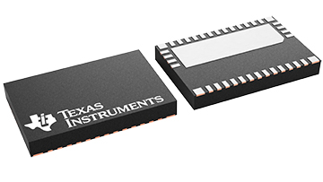
The LMG3624 is a 650V 170mΩ GaN power FET intended for switch-mode power-supply applications. The LMG3624 simplifies design and reduces component count by integrating the GaN FET and gate driver in a 8mm by 5.3mm QFN package.

Programmable turn-on slew rates provide EMI and ringing control. The current-sense emulation reduces power dissipation compared to the traditional current-sense resistor and allows the low-side thermal pad to be connected to the cooling PCB power ground.

The LMG3624 supports converter light-load efficiency requirements and burst-mode operation with low quiescent currents and fast start-up times. Protection features include under-voltage lockout (UVLO), cycle-by-cycle current limit, and overtemperature protection. Overtemperature protection is reported with the open-drain FLT pin.
Package Information
PART NUMBER PACKAGE(1) PACKAGE SIZE(2)
LMG3624 REQ (VQFN, 38) 8mm × 5.3mm
For more information, see the Mechanical, Packaging, and Orderable Information section.
The package size (length × width) is a nominal value and includes pins, where applicable.

LMG3624 38-Pin VQFN

38-Pin VQFN