SNOSDL9 December 2024 LMG5126
ADVANCE INFORMATION
- 1
- 1 Features
- 2 Applications
- 3 Description
- 4 Pin Configuration and Functions
- 5 Specifications
- 6 Detailed Description
- 7 Application and Implementation
- 8 Device and Documentation Support
- 9 Revision History
- 10Mechanical, Packaging, and Orderable Information
Package Options
Mechanical Data (Package|Pins)
- VBT|22
Thermal pad, mechanical data (Package|Pins)
Orderable Information
6.3.3 Dual Random Spread Spectrum (DRSS)
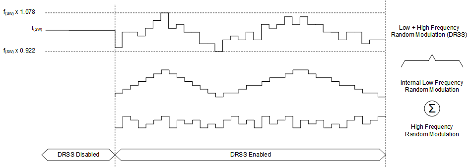
The device provides a digital spread spectrum, which reduces the EMI of the power supply over a wide frequency range. This function can be enabled by the CFG1-pin. When the spread spectrum is enabled, the internal modulator dithers the internal clock. When the device is configured to use an external clock applied at the SYNCIN-pin, the internal spread spectrum is disabled. DRSS combines a low frequency triangular modulation profile with a high frequency cycle-by-cycle random modulation profile. The low frequency triangular modulation improves performance in lower radio frequency bands (for example AM band), while the high frequency random modulation improves performance in higher radio frequency bands (for example FM band). In addition, the frequency of the triangular modulation is further modulated randomly to reduce the likelihood of any audible tones. To minimize output voltage ripple caused by spread spectrum, duty cycle is modified on a cycle-by-cycle basis to maintain a nearly constant duty cycle when dithering is enabled.
 Figure 6-2 Dual Random Spread
Spectrum