SNLS270L August 2007 – January 2016 LMH0356
PRODUCTION DATA.
- 1 Features
- 2 Applications
- 3 Description
- 4 Revision History
- 5 Description (continued)
- 6 Pin Configuration and Functions
- 7 Specifications
- 8 Detailed Description
- 9 Application and Implementation
- 10Power Supply Recommendations
- 11Layout
- 12Device and Documentation Support
- 13Mechanical, Packaging, and Orderable Information
Package Options
Mechanical Data (Package|Pins)
Thermal pad, mechanical data (Package|Pins)
- RHS|48
Orderable Information
11 Layout
11.1 Layout Guidelines
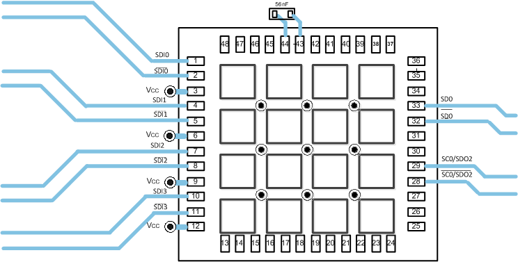
Figure 11 shows a typical PCB layout for the 48-pin WQFN version of the LMH0356. The following guidelines are recommended for designing the board layout for the LMH0356:
- Choose a suitable board stack-up such that it supports 100-Ω differential trace routing on board layer 1. This is typically done with layer 2 ground plane reference for the 100-Ω differential traces.
- Place 56-nF loop filter capacitor as close to the loop filter pins as possible.
- Use coupled differential traces with 100-Ω ± 5% impedance for signal routing to SDI± and SDO± pins. These are usually 5 to 8-mil trace width reference to a ground plane at layer 2.
- DAP of the package must be connected to the ground plane through an array of via. These nine vias are solder-masked to avoid solder flowing into the plated-through holes during the board manufacturing process. DAP is divided into 16 squares (1.09 mm × 1.09 mm) inside 5.1-mm × 5.1-mm landing pad.
- Connect supply pins VCC and VEE to the power and ground planes with short via. The via is usually placed tangent to the supply pin landing pad with the shortest trace possible.
- Power supply bypass capacitors must be placed close to the supply pin. They are commonly placed at the bottom layer sharing the ground connector of the DAP.
11.2 Layout Example
Figure 11 shows a typical PCB layout for the 48-pin WQFN version of the LMH0356.
 Figure 11. LMH0356 PCB Layout Example