SNLS308G April   2009  – June 2015 LMH0384

PRODUCTION DATA.  

  1. Features
  2. Applications
  3. Description
  4. Revision History
  5. Pin Configuration and Functions
  6. Specifications
    1. 6.1 Absolute Maximum Ratings
    2. 6.2 ESD Ratings
    3. 6.3 Recommended Operating Conditions
    4. 6.4 Thermal Information
    5. 6.5 DC Electrical Characteristics
    6. 6.6 AC Electrical Characteristics
    7. 6.7 Timing Requirements
    8. 6.8 Switching Characteristics
    9. 6.9 Typical Characteristics
  7. Detailed Description
    1. 7.1 Overview
    2. 7.2 Functional Block Diagram
    3. 7.3 Feature Description
      1. 7.3.1 Block Description
      2. 7.3.2 Mute Reference (MUTEREF)
      3. 7.3.3 Carrier Detect (CD) and Mute
      4. 7.3.4 Auto Sleep
      5. 7.3.5 Input Interfacing
      6. 7.3.6 Output Interfacing
    4. 7.4 Device Functional Modes
    5. 7.5 Programming
      1. 7.5.1 SPI Write
      2. 7.5.2 SPI Read
      3. 7.5.3 Output Driver Adjustments
      4. 7.5.4 Launch Amplitude Optimization
      5. 7.5.5 Cable Length Indicator (CLI)
      6. 7.5.6 Application of CLI: Extending 3G Reach
      7. 7.5.7 Explanation of Extended 3G Reach Mode State Machine ()
    6. 7.6 Register Maps
  8. Application and Implementation
    1. 8.1 Application Information
      1. 8.1.1 Replacing the LMH0344
    2. 8.2 Typical Application
      1. 8.2.1 Design Requirements
      2. 8.2.2 Detailed Design Procedure
      3. 8.2.3 Application Curves
    3. 8.3 Dos and Don'ts
  9. Power Supply Recommendations
  10. 10Layout
    1. 10.1 Layout Guidelines
    2. 10.2 Layout Example
  11. 11Device and Documentation Support
    1. 11.1 Documentation Support
      1. 11.1.1 Related Documentation
    2. 11.2 Community Resources
    3. 11.3 Trademarks
    4. 11.4 Electrostatic Discharge Caution
    5. 11.5 Glossary
  12. 12Mechanical, Packaging, and Orderable Information

Package Options

Mechanical Data (Package|Pins)
Thermal pad, mechanical data (Package|Pins)
Orderable Information

5 Pin Configuration and Functions

RUM Package
16-Pin WQFN
Top View
LMH0384 30083003.gif

NOTE:

The exposed die attach pad is a negative electrical terminal for this device. It should be connected to the negative power supply voltage.

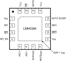
Pin Functions – Pin Mode (non-SPI) / SPI_EN = GND / LMH0344 Compatible

PIN I/O, TYPE DESCRIPTION
NO. NAME
1 VEE Ground Negative power supply (ground).
2 SDI I, SDI Serial data true input.
3 SDI I, SDI Serial data complement input.
4 SPI_EN I, LVCMOS SPI register access enable. This pin has an internal pulldown.
H = SPI register access mode.
L = Pin mode.
5 AEC+ I/O, Analog AEC loop filter external capacitor (1-µF) positive connection.
6 AEC- I/O, Analog AEC loop filter external capacitor (1-µF) negative connection.
7 BYPASS I, LVCMOS Equalization bypass. This pin has an internal pulldown.
H = Equalization is bypassed (no equalization occurs).
L = Normal operation.
8 MUTEREF I, Analog Mute reference input. Sets the threshold for CD and (with CD tied to MUTE) determines the maximum cable to be equalized before muting. MUTEREF may be either unconnected or connected to ground for normal CD operation.
9 VEE I, LVCMOS Connect this pin to ground or drive it logic low.
10 SDO O, LVDS Serial data complement output.
11 SDO O, LVDS Serial data true output.
12 AUTO SLEEP I, LVCMOS Auto Sleep. AUTO SLEEP has precedence over MUTE and BYPASS. This pin has an internal pullup.
H = Device will power down when no input is detected.
L = Normal operation (device will not enter auto power down).
13 VCC Power Positive power supply (+3.3 V).
14 MUTE I, LVCMOS Output mute. CD may be tied to this pin to inhibit the output when no input signal is present. MUTE has precedence over BYPASS. This pin has an internal pulldown.
H = Outputs forced to a muted state (logic zero).
L = Outputs enabled.
15 CD O, LVCMOS Carrier detect.
H = No input signal detected.
L = Input signal detected.
16 VCC Power Positive power supply (+3.3 V).
VEE Ground Connect exposed DAP to negative power supply (ground).
RUM Package
16-Pin WQFN
Top View
LMH0384 30083007.gif

NOTE:

The exposed die attach pad is a negative electrical terminal for this device. It should be connected to the negative power supply voltage.

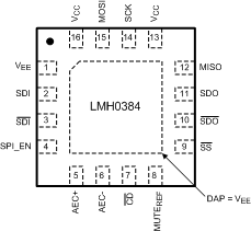
Pin Functions – SPI Mode / SPI_EN = VCC

PIN I/O, TYPE DESCRIPTION
NO. NAME
1 VEE Ground Negative power supply (ground).
2 SDI I, SDI Serial data true input.
3 SDI I, SDI Serial data complement input.
4 SPI_EN I, LVCMOS SPI register access enable. This pin has an internal pulldown.
H = SPI register access mode.
L = Pin mode.
5 AEC+ I/O, Analog AEC loop filter external capacitor (1 µF) positive connection.
6 AEC- I/O, Analog AEC loop filter external capacitor (1 µF) negative connection.
7 CD O, LVCMOS Carrier detect.
H = No input signal detected.
L = Input signal detected.
8 MUTEREF I, Analog Mute reference input. Sets the threshold for CD and (with CD tied to MUTE) determines the maximum cable to be equalized before muting. MUTEREF may be either unconnected or connected to ground for normal CD operation.
9 SS (SPI) I, LVCMOS SPI slave select. This pin has an internal pullup.
10 SDO O, LVDS Serial data complement output.
11 SDO O, LVDS Serial data true output.
12 MISO (SPI) O, LVCMOS SPI Master Input / Slave Output. LMH0384 data transmit.
13 VCC Power Positive power supply (+3.3 V).
14 SCK (SPI) I, LVCMOS SPI serial clock input.
15 MOSI (SPI) I, LVCMOS SPI Master Output / Slave Input. LMH0384 data receive.
16 VCC Power Positive power supply (+3.3 V).
VEE Ground Connect exposed DAP to negative power supply (ground).