SNLS312M August 2010 – July 2015 LMH0394
PRODUCTION DATA.
- 1 Features
- 2 Applications
- 3 Description
- 4 Revision History
- 5 Pin Configuration and Functions
- 6 Specifications
-
7 Detailed Description
- 7.1 Overview
- 7.2 Functional Block Diagram
- 7.3 Feature Description
- 7.4 Device Functional Modes
- 7.5
Programming
- 7.5.1
SPI Register Access
- 7.5.1.1 SPI Transaction Overview
- 7.5.1.2 SPI Write
- 7.5.1.3 SPI Read
- 7.5.1.4 SPI Daisy-Chain Operation
- 7.5.1.5 SPI Daisy-Chain Write
- 7.5.1.6 SPI Daisy-Chain Read
- 7.5.1.7 SPI Daisy-Chain Read and Write Example
- 7.5.1.8 SPI Daisy-Chain Length Detection
- 7.5.1.9 Output Driver Adjustments and De-emphasis Setting
- 7.5.1.10 Launch Amplitude Optimization
- 7.5.1.11 Cable Length Indicator (CLI)
- 7.5.1
SPI Register Access
- 7.6 Register Maps
- 8 Application and Implementation
- 9 Power Supply Recommendations
- 10Layout
- 11Device and Documentation Support
- 12Mechanical, Packaging, and Orderable Information
Package Options
Mechanical Data (Package|Pins)
- RUM|16
Thermal pad, mechanical data (Package|Pins)
- RUM|16
Orderable Information
5 Pin Configuration and Functions
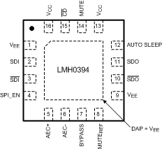
RUM Package
16-Pin WQFN (Non-SPI)
Top View

Pin Functions – Pin Mode (non-SPI) / SPI_EN = GND / LMH0344 Compatible
| PIN | I/O, TYPE | DESCRIPTION | |
|---|---|---|---|
| NO. | NAME | ||
| 1 | VEE | Ground | Negative power supply (ground). |
| 2 | SDI | I, Analog | Serial data true input. |
| 3 | SDI | I, Analog | Serial data complement input. |
| 4 | SPI_EN | I, LVCMOS | SPI register access enable. This pin has an internal pulldown. H = SPI register access mode. L = Pin mode. |
| 5 | AEC+ | I/O, Analog | AEC loop filter external capacitor (1-µF) positive connection (capacitor is optional). |
| 6 | AEC- | I/O, Analog | AEC loop filter external capacitor (1-µF) negative connection (capacitor is optional). |
| 7 | BYPASS | I, LVCMOS | Equalization bypass. This pin has an internal pull-down. H = Equalization is bypassed (no equalization occurs). L = Normal operation. |
| 8 | MUTEREF | I, Analog | Mute reference input. Sets the threshold for CD and (with CD tied to MUTE) determines the maximum cable to be equalized before muting. MUTEREF may be either unconnected or connected to ground for normal CD operation. |
| 9 | VEE | I, LVCMOS | Connect this pin to ground or drive it logic low. |
| 10 | SDO | O, LVDS | Serial data complement output. |
| 11 | SDO | O, LVDS | Serial data true output. |
| 12 | AUTO SLEEP | I, LVCMOS | Auto Sleep. AUTO SLEEP has precedence over MUTE and BYPASS. This pin has an internal pullup. H = Device will power down when no input is detected. L = Normal operation (device will not enter auto power down). |
| 13 | VCC | Power | Positive power supply (+2.5 V). |
| 14 | MUTE | I, LVCMOS | Output mute. CD may be tied to this pin to inhibit the output when no input signal is present. MUTE has precedence over BYPASS. This pin has an internal pull-down. H = Outputs forced to a muted state. L = Outputs enabled. |
| 15 | CD | O, LVCMOS | Carrier detect. H = No input signal detected. L = Input signal detected. |
| 16 | VCC | Power | Positive power supply (2.5 V). |
| DAP | VEE | Ground | Connect exposed DAP to negative power supply (ground). See Figure 22 for layout example. |
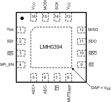
RUM Package
16-Pin WQFN (SPI)
Top View

Pin Functions – SPI Mode / SPI_EN = VCC
| PIN | I/O, TYPE | DESCRIPTION | |
|---|---|---|---|
| NO. | NAME | ||
| 1 | VEE | Ground | Negative power supply (ground). |
| 2 | SDI | I, Analog | Serial data true input. |
| 3 | SDI | I, Analog | Serial data complement input. |
| 4 | SPI_EN | I, LVCMOS | SPI register access enable. This pin has an internal pull-down. H = SPI register access mode. L = Pin mode. |
| 5 | AEC+ | I/O, Analog | AEC loop filter external capacitor (1 µF) positive connection (capacitor is optional). |
| 6 | AEC- | I/O, Analog | AEC loop filter external capacitor (1 µF) negative connection (capacitor is optional). |
| 7 | CD | O, LVCMOS | Carrier detect. H = No input signal detected. L = Input signal detected. |
| 8 | MUTEREF | I, Analog | Mute reference input. Sets the threshold for CD and (with CD tied to MUTE) determines the maximum cable to be equalized before muting. MUTEREF may be either unconnected or connected to ground for normal CD operation. |
| 9 | SS (SPI) | I, LVCMOS | SPI slave select. This pin has an internal pullup. |
| 10 | SDO | O, LVDS | Serial data complement output. |
| 11 | SDO | O, LVDS | Serial data true output. |
| 12 | MISO (SPI) | O, LVCMOS | SPI Master Input / Slave Output. LMH0394 control data transmit. |
| 13 | VCC | Power | Positive power supply (2.5 V). |
| 14 | SCK (SPI) | I, LVCMOS | SPI serial clock input. |
| 15 | MOSI (SPI) | I, LVCMOS | SPI Master Output / Slave Input. LMH0394 control data receive. This pin has an internal pulldown. |
| 16 | VCC | Power | Positive power supply (2.5 V). |
| DAP | VEE | Ground | Connect exposed DAP to negative power supply (ground). See Figure 22 for layout example. |