SNLS534D April   2016  – June 2018 LMH1226

PRODUCTION DATA.  

  1. Features
  2. Applications
  3. Description
    1.     Device Images
      1.      Simplified Block Diagram
  4. Revision History
  5. Pin Configuration and Functions
    1.     Pin Functions
  6. Specifications
    1. 6.1 Absolute Maximum Ratings
    2. 6.2 ESD Ratings
    3. 6.3 Recommended Operating Conditions
    4. 6.4 Thermal Information
    5. 6.5 Electrical Characteristics
    6. 6.6 Recommended SMBus Interface AC Timing Specifications
    7. 6.7 Serial Parallel Interface (SPI) AC Timing Specifications
    8. 6.8 Typical Characteristics
  7. Detailed Description
    1. 7.1 Overview
    2. 7.2 Functional Block Diagram
    3. 7.3 Feature Description
      1. 7.3.1 4-Level Input Configuration Pins
      2. 7.3.2 Input Carrier Detect
      3. 7.3.3 Continuous Time Linear Equalizer (CTLE)
        1. 7.3.3.1 Adaptive PCB Trace Equalizer (IN1±)
      4. 7.3.4 Input-Output Mux Selection
      5. 7.3.5 Clock and Data Recovery (CDR) Reclocker
      6. 7.3.6 Internal Eye Opening Monitor (EOM)
      7. 7.3.7 Output Function Control
      8. 7.3.8 Output Driver Amplitude and De-Emphasis Control
      9. 7.3.9 Status Indicators and Interrupts
        1. 7.3.9.1 LOCK_N (Lock Indicator)
        2. 7.3.9.2 CD_N (Carrier Detect)
        3. 7.3.9.3 INT_N (Interrupt)
    4. 7.4 Device Functional Modes
      1. 7.4.1 System Management Bus (SMBus) Mode
        1. 7.4.1.1 SMBus Read and Write Transactions
          1. 7.4.1.1.1 SMBus Write Operation Format
          2. 7.4.1.1.2 SMBus Read Operation Format
      2. 7.4.2 Serial Peripheral Interface (SPI) Mode
        1. 7.4.2.1 SPI Read and Write Transactions
          1. 7.4.2.1.1 SPI Write Transaction Format
          2. 7.4.2.1.2 SPI Read Transaction Format
        2. 7.4.2.2 SPI Daisy Chain
    5. 7.5 LMH1226 Register Map
      1. 7.5.1 Share Register Page
      2. 7.5.2 CTLE/CDR Register Page
      3. 7.5.3 Drivers Register Page
  8. Application and Implementation
    1. 8.1 Application Information
      1. 8.1.1 General Guidance for SMPTE and 10 GbE Applications
      2. 8.1.2 LMH1219 and LMH1226 Compatibility
    2. 8.2 Typical Application
      1. 8.2.1 Design Requirements
      2. 8.2.2 Detailed Design Procedure
      3. 8.2.3 Recommended VOD and DEM Register Settings
      4. 8.2.4 Application Performance Plots
  9. Power Supply Recommendations
  10. 10Layout
    1. 10.1 PCB Layout Guidelines
    2. 10.2 Layout Example
  11. 11Device and Documentation Support
    1. 11.1 Receiving Notification of Documentation Updates
    2. 11.2 Community Resources
    3. 11.3 Trademarks
    4. 11.4 Electrostatic Discharge Caution
    5. 11.5 Glossary
  12. 12Mechanical, Packaging, and Orderable Information

Package Options

Mechanical Data (Package|Pins)
Thermal pad, mechanical data (Package|Pins)
Orderable Information

SMBus Read Operation Format

Reading data from a slave device consists of four parts, as illustrated in Figure 17:

  1. The master begins with a start condition, followed by the slave device address with the R/W bit set to 0'b.
  2. After an ACK from the slave device, the 8-bit register word address is written.
  3. After an ACK from the slave device, the master initiates a re-start condition, followed by the slave address with the R/W bit set to 1'b.
  4. After an ACK from the slave device, the 8-bit data is read back. The last ACK is high if there are no more bytes to read, and the last read is followed by a stop condition.
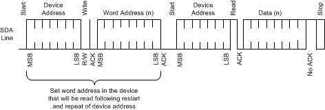
LMH1226 smbus_read_operation_snls515.gifFigure 17. SMBus Read Operation