SNWS020C November 2007 – October 2015 LMH2100
PRODUCTION DATA.
- 1 Features
- 2 Applications
- 3 Description
- 4 Revision History
- 5 Pin Configuration and Functions
- 6 Specifications
- 7 Detailed Description
- 8 Application and Implementation
- 9 Power Supply Recommendations
- 10Layout
- 11Device and Documentation Support
- 12Mechanical, Packaging, and Orderable Information
Package Options
Mechanical Data (Package|Pins)
- YFQ|6
Thermal pad, mechanical data (Package|Pins)
Orderable Information
7 Detailed Description
7.1 Overview
The LMH2100 is a versatile logarithmic RF power detector suitable for use in power measurement systems. The LMH2100 is particularly well suited for CDMA and UMTS applications. It produces a DC voltage that is a measure for the applied RF power.
The core of the LMH2100 is a progressive compression LOG detector consisting of four gain stages. Each of these saturating stages has a gain of approximately 10 dB and therefore realizes about 10 dB of the detector dynamic range. The five diode cells perform the actual detection and convert the RF signal to a DC current. This DC current is subsequently supplied to the transimpedance amplifier at the output, that converts it into an output voltage. In addition, the amplifier provides buffering of and applies filtering to the detector output signal. To prevent discharge of filtering capacitors between OUT and GND in shutdown, a switch is inserted at the amplifier input that opens in shutdown to realize a high impedance output of the device.
7.2 Functional Block Diagram
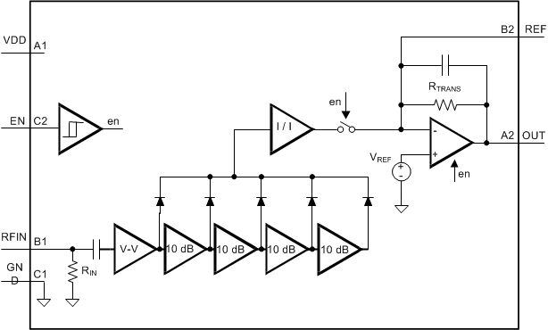
7.3 Feature Description
7.3.1 Characteristics of the LMH2100
The LMH2100 is a logarithmic RF power detector with approximately 40-dB dynamic range. This dynamic range plus its logarithmic behavior make the LMH2100 ideal for various applications such as wireless transmit power control for CDMA and UMTS applications. The frequency range of the LMH2100 is from 50 MHz to 4 GHz, which makes it suitable for various applications.
The LMH2100 transfer function is accurately temperature compensated. This makes the measurement accurate for a wide temperature range. Furthermore, the LMH2100 can easily be connected to a directional coupler because of its 50-Ω input termination. The output range is adjustable to fit the ADC input range. The detector can be switched into a power saving shutdown mode for use in pulsed conditions.
7.3.2 Accurate Power Measurement
The power measurement accuracy achieved with a power detector is not only determined by the accuracy of the detector itself, but also by the way it is integrated into the application. In many applications some form of calibration is employed to improve the accuracy of the overall system beyond the intrinsic accuracy provided by the power detector. For example, for LOG-detectors calibration can be used to eliminate part to part spread of the LOG-slope and LOG-intercept from the overall power measurement system, thereby improving its power measurement accuracy.
This section shows how calibration techniques can be used to improve the accuracy of a power measurement system beyond the intrinsic accuracy of the power detector itself. The main focus of the section is on power measurement systems using LOG-detectors, specifically the LMH2100, but the more generic concepts can also be applied to other power detectors. Other factors influencing the power measurement accuracy, such as the resolution of the ADC reading the detector output signal will not be considered here since they are not fundamentally due to the power detector.
7.3.2.1 LOG-Conformance Error
Probably the simplest power measurement system that can be realized is obtained when the LOG-detector transfer function is modelled as a perfect linear-in-dB relationship between the input power and output voltage:

in which KSLOPE represents the LOG-slope and PINTERCEPT the LOG-intercept. The estimator based on this model implements the inverse of the model equation, that is:

The resulting power measurement error, the LOG-conformance error, is thus equal to:

The most important contributions to the LOG-conformance error are generally:
- The deviation of the actual detector transfer function from an ideal Logarithm (the transfer function is nonlinear in dB).
- Drift of the detector transfer function over various environmental conditions, most importantly temperature; KSLOPE and PINTERCEPT are usually determined for room temperature only.
- Part-to-part spread of the (room temperature) transfer function.
The latter component is conveniently removed by means of calibration, that is, if the LOG slope and LOG-intercept are determined for each individual detector device (at room temperature). This can be achieved by measurement of the detector output voltage - at room temperature - for a series of different power levels in the LOG-linear range of the detector transfer function. The slope and intercept can then be determined by means of linear regression.
An example of this type of error and its relationship to the detector transfer function is depicted in Figure 71.
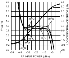 Figure 71. LOG-Conformance Error and LOG-Detector Transfer Function
In the center of the detector's dynamic range, the LOG-conformance error is small, especially at room temperature; in this region the transfer function closely follows the linear-in-dB relationship while KSLOPE and PINTERCEPT are determined based on room temperature measurements. At the temperature extremes the error in the center of the range is slightly larger due to the temperature drift of the detector transfer function. The error rapidly increases toward the top and bottom end of the detector's dynamic range; here the detector saturates and its transfer function starts to deviate significantly from the ideal LOG-linear model. The detector dynamic range is usually defined as the power range for which the LOG conformance error is smaller than a specified amount. Often an error of ±1 dB is used as a criterion.
7.3.2.2 Temperature Drift Error
A more accurate power measurement system can be obtained if the first error contribution, due to the deviation from the ideal LOG-linear model, is eliminated. This is achieved if the actual measured detector transfer function at room temperature is used as a model for the detector, instead of the ideal LOG-linear transfer function used in the previous section.
The formula used for such a detector is:
where
- TO represents the temperature during calibration (room temperature).
The transfer function of the corresponding estimator is thus the inverse of this:

In this expression VOUT(T) represents the measured detector output voltage at the operating temperature T.
The resulting measurement error is only due to drift of the detector transfer function over temperature, and can be expressed as:

Unfortunately, the (numeric) inverse of the detector transfer function at different temperatures makes this expression rather impractical. However, since the drift error is usually small VOUT(T) is only slightly different from VOUT(TO). This means that we can apply the following approximation:

This expression is easily simplified by taking the following considerations into account:
- The drift error at the calibration temperature E(TO,TO) equals zero (by definition).
- The estimator transfer FDET(VOUT,TO) is not a function of temperature; the estimator output changes over temperature only due to the temperature dependence of VOUT.
- The actual detector input power PIN is not temperature dependent (in the context of this expression).
- The derivative of the estimator transfer function to VOUT equals approximately 1/KSLOPE in the LOG-linear region of the detector transfer function (the region of interest).
Using this, we arrive at:

This expression is very similar to the expression of the LOG-conformance error determined previously. The only difference is that instead of the output of the ideal LOG-linear model, the actual detector output voltage at the calibration temperature is now subtracted from the detector output voltage at the operating temperature.
Figure 72 depicts an example of the drift error.
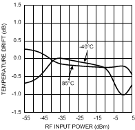 Figure 72. Temperature Drift Error of the LMH2100 at ƒ = 1855 MHz
In agreement with the definition, the temperature drift error is zero at the calibration temperature. Further, the main difference with the LOG-conformance error is observed at the top and bottom end of the detection range; instead of a rapid increase the drift error settles to a small value at high and low input power levels due to the fact that the detector saturation levels are relatively temperature independent.
In a practical application it may not be possible to use the exact inverse detector transfer function as the algorithm for the estimator. For example it may require too much memory and/or too much factory calibration time. However, using the ideal LOG-linear model in combination with a few extra data points at the top and bottom end of the detection range - where the deviation is largest - can already significantly reduce the power measurement error.
7.3.2.2.1 Temperature Compensation
A further reduction of the power measurement error is possible if the operating temperature is measured in the application. For this purpose, the detector model used by the estimator should be extended to cover the temperature dependency of the detector.
Since the detector transfer function is generally a smooth function of temperature (the output voltage changes gradually over temperature), the temperature is in most cases adequately modeled by a first-order or second-order polynomial (see Equation 9).

The required temperature dependence of the estimator, to compensate for the detector temperature dependence can be approximated similarly:

The last approximation results from the fact that a first-order temperature compensation is usually sufficiently accurate. The remainder of this section will therefore concentrate on first-order compensation. For second and higher-order compensation a similar approach can be followed.
Ideally, the temperature drift could be completely eliminated if the measurement system is calibrated at various temperatures and input power levels to determine the Temperature Sensitivity S1. In a practical application, however that is usually not possible due to the associated high costs. The alternative is to use the average temperature drift in the estimator, instead of the temperature sensitivity of each device individually. In this way it becomes possible to eliminate the systematic (reproducible) component of the temperature drift without the need for calibration at different temperatures during manufacturing. What remains is the random temperature drift, which differs from device to device. Figure 73 illustrates the idea. The graph at the left schematically represents the behavior of the drift error versus temperature at a certain input power level for a large number of devices.
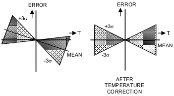 Figure 73. Elimination of the Systematic Component from the Temperature Drift
The mean drift error represents the reproducible - systematic - part of the error, while the mean ± 3 sigma limits represent the combined systematic plus random error component. Obviously the drift error must be zero at calibration temperature T0. If the systematic component of the drift error is included in the estimator, the total drift error becomes equal to only the random component, as illustrated in the graph at the right of Figure 73. A significant reduction of the temperature drift error can be achieved in this way only if:
- The systematic component is significantly larger than the random error component (otherwise the difference is negligible).
- The operating temperature is measured with sufficient accuracy.
It is essential for the effectiveness of the temperature compensation to assign the appropriate value to the temperature sensitivity S1. Two different approaches can be followed to determine this parameter:
- Determination of a single value to be used over the entire operating temperature range.
- Division of the operating temperature range in segments and use of separate values for each of the segments.
Also for the first method, the accuracy of the extracted temperature sensitivity increases when the number of measurement temperatures increases. Linear regression to temperature can then be used to determine the two parameters of the linear model for the temperature drift error: the first order temperature sensitivity S1 and the best-fit (room temperature) value for the power estimate at T0: FDET[VOUT(T),T0]. Note that to achieve an overall - over all temperatures - minimum error, the room temperature drift error in the model can be non-zero at the calibration temperature (which is not in agreement with the strict definition).
The second method does not have this drawback but is more complex. In fact, segmentation of the temperature range is a form of higher-order temperature compensation using only a first-order model for the different segments: one for temperatures below 25°C, and one for temperatures above 25°C. The mean (or typical) temperature sensitivity is the value to be used for compensation of the systematic drift error component. Figure 75 shows the temperature drift error without and with temperature compensation using two segments. With compensation the systematic component is completely eliminated; the remaining random error component is centered around zero. Note that the random component is slightly larger at −40°C than at 85°C.
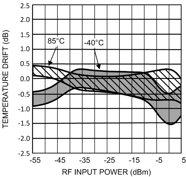 Figure 74. Temperature Drift Error without Temperature Compensation
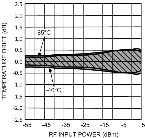 Figure 75. Temperature Drift Error without with Temperature Compensation
In a practical power measurement system, temperature compensation is usually only applied to a small power range around the maximum power level for two reasons:
- The various communication standards require the highest accuracy in this range to limit interference.
- The temperature sensitivity itself is a function of the power level it becomes impractical to store a large number of different temperature sensitivity values for different power levels.
The 2.7-V DC and AC Electrical Characteristics in the datasheet specifies the temperature sensitivity for the aforementioned two segments at an input power level of −10 dBm (near the top-end of the detector dynamic range). The typical value represents the mean which is to be used for calibration.
7.3.2.2.2 Differential Power Errors
Many third generation communication systems contain a power control loop through the base station and mobile unit that requests both to frequently update the transmit power level by a small amount (typically 1 dB). For such applications it is important that the actual change of the transmit power is sufficiently close to the requested power change.
The error metrics in the datasheet that describe the accuracy of the detector for a change in the input power are E1 dB (for a 1-dB change in the input power) and E10 dB (for a 10-dB step, or ten consecutive steps of 1 dB). Since it can be assumed that the temperature does not change during the power step the differential error equals the difference of the drift error at the two involved power levels:

It should be noted that the step error increases significantly when one (or both) power levels in the above expression are outside the detector dynamic range. For E10 dB this occurs when PIN is less than 10 dB below the maximum input power of the dynamic range, PMAX.
7.4 Device Functional Modes
7.4.1 Shutdown
To save power, the LMH2100 can be brought into a low-power shutdown mode. The device is active for EN = HIGH (VEN>1.1 V) and in the low-power shutdown mode for EN = LOW (VEN < 0.6 V). In this state the output of the LMH2100 is switched to a high impedance mode. Using the shutdown function, care must be taken not to exceed the absolute maximum ratings. Forcing a voltage to the enable input that is 400 mV higher than VDD or 400 mV lower than GND will damage the device and further operations is not ensured. The absolute maximum ratings can also be exceeded when the enable EN is switched to HIGH (from shutdown to active mode) while the supply voltage is low (off). This should be prevented at all times. A possible solution to protect the part is to add a resistor of 100 kΩ in series with the enable input.
7.4.1.1 Output Behavior in Shutdown
In order to save power, the LMH2100 can be used in pulsed mode, such that it is active to perform the power measurement only during a fraction of the time. During the remaining time the device is in low-power shutdown. Applications using this approach usually require that the output value is available at all times, also when the LMH2100 is in shutdown. The settling time in active mode, however, should not become excessively large. This can be realized by the combination of the LMH2100 and a low pass output filter (see Figure 81).
In active mode, the filter capacitor CS is charged to the output voltage of the LMH2100, which in this mode has a low output impedance to enable fast settling. During shutdown-mode, the capacitor should preserve this voltage. Discharge of CS through any current path should therefore be avoided in shutdown. The output impedance of the LMH2100 becomes high in shutdown, such that the discharge current cannot flow from the capacitor top plate, through RS, and the LMH2100 devices's OUT pin to GND. This is realized by the internal shutdown mechanism of the output amplifier and by the switch depicted in Figure 85. Additionally, it should be ensured that the ADC input impedance is high as well, to prevent a possible discharge path through the ADC.