SNWS020C November   2007  – October 2015 LMH2100

PRODUCTION DATA.  

  1. Features
  2. Applications
  3. Description
  4. Revision History
  5. Pin Configuration and Functions
  6. Specifications
    1. 6.1 Absolute Maximum Ratings
    2. 6.2 ESD Ratings
    3. 6.3 Recommended Operating Ratings
    4. 6.4 Thermal Information
    5. 6.5 2.7-V DC and AC Electrical Characteristics
    6. 6.6 Timing Requirements
    7. 6.7 Typical Characteristics
  7. Detailed Description
    1. 7.1 Overview
    2. 7.2 Functional Block Diagram
    3. 7.3 Feature Description
      1. 7.3.1 Characteristics of the LMH2100
      2. 7.3.2 Accurate Power Measurement
        1. 7.3.2.1 LOG-Conformance Error
        2. 7.3.2.2 Temperature Drift Error
          1. 7.3.2.2.1 Temperature Compensation
          2. 7.3.2.2.2 Differential Power Errors
    4. 7.4 Device Functional Modes
      1. 7.4.1 Shutdown
        1. 7.4.1.1 Output Behavior in Shutdown
  8. Application and Implementation
    1. 8.1 Application Information
      1. 8.1.1 Functionality and Application of RF Power Detectors
        1. 8.1.1.1 Functionality of RF Power Detectors
          1. 8.1.1.1.1 Key Characteristics of RF Power Detectors
          2. 8.1.1.1.2 Types of RF Power Detectors
            1. 8.1.1.1.2.1 Diode Detector
            2. 8.1.1.1.2.2 (Root) Mean Square Detector
            3. 8.1.1.1.2.3 Logarithmic Detectors
    2. 8.2 Typical Applications
      1. 8.2.1 Application With Transmit Power Control Loop
        1. 8.2.1.1 Design Requirements
        2. 8.2.1.2 Detailed Design Procedure
          1. 8.2.1.2.1 Detector Interfacing
            1. 8.2.1.2.1.1 Concept of Power Measurements
            2. 8.2.1.2.1.2 RF Input
            3. 8.2.1.2.1.3 Output and Reference
              1. 8.2.1.2.1.3.1 Filtering
            4. 8.2.1.2.1.4 Interface to the ADC
        3. 8.2.1.3 Application Curves
      2. 8.2.2 Application With Voltage Standing Wave Ratio Measurement
  9. Power Supply Recommendations
  10. 10Layout
    1. 10.1 Layout Guidelines
      1. 10.1.1 Supply Lines
        1. 10.1.1.1 Positive Supply (VDD)
        2. 10.1.1.2 Ground (GND)
      2. 10.1.2 RF Input Interface
      3. 10.1.3 Microstrip Configuration
      4. 10.1.4 GCPW Configuration
      5. 10.1.5 Reference (REF)
      6. 10.1.6 Output (OUT)
    2. 10.2 Layout Example
  11. 11Device and Documentation Support
    1. 11.1 Community Resources
    2. 11.2 Trademarks
    3. 11.3 Electrostatic Discharge Caution
    4. 11.4 Glossary
  12. 12Mechanical, Packaging, and Orderable Information

Package Options

Mechanical Data (Package|Pins)
Thermal pad, mechanical data (Package|Pins)
Orderable Information

5 Pin Configuration and Functions

YFQ Package
6-Pin DSBGA
Top View
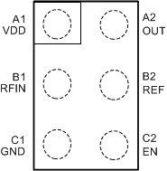
LMH2100 30014002.gif

Pin Functions

PIN I/O DESCRIPTION
NUMBER NAME
A1 VDD Power Supply Positive supply voltage
A2 OUT Output Ground referenced detector output voltage (linear in dB)
B1 RFIN Analog Input RF input signal to the detector, internally terminated with 50 Ω.
B2 REF Reference Output Reference output, for differential output measurement (without pedestal). Connected to inverting input of output amplifier.
C1 GND GND Power ground
C2 EN Logic Input The device is enabled for EN = High, and brought to a low-power shutdown mode for EN = Low.