SNWS022D January 2010 – June 2015 LMH2110
PRODUCTION DATA.
- 1 Features
- 2 Applications
- 3 Description
- 4 Revision History
- 5 Pin Configuration and Functions
- 6 Specifications
- 7 Detailed Description
-
8 Application and Implementation
- 8.1 Application Information
- 8.2 Typical Applications
- 9 Power Supply Recommendations
- 10Layout
- 11Device and Documentation Support
- 12Mechanical, Packaging, and Orderable Information
Package Options
Mechanical Data (Package|Pins)
- YFQ|6
Thermal pad, mechanical data (Package|Pins)
Orderable Information
7 Detailed Description
7.1 Overview
The LMH2110 is a high-performance logarithmic root mean square (RMS) power detector which measures the actual power content of a signal. The device has a RF input power detection range from –40 dBm to 5 dBm and provides accurate output voltage that relates linearly to the RF input power in dBm. This output voltage exhibits high temperature insensitivity ranging ±0.25 dB.
The device has an internal low dropout linear regulator (LDO) making the device insensitive to input supply variation and allowing operation from a wide input supply range from 2.7 V to 5 V. Additional features include multi-band operation from 50 MHz to 8 GHz, shutdown functionality to save power, and minimal slope and intercept variation.
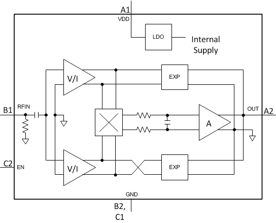
7.2 Functional Block Diagram

7.3 Feature Description
7.3.1 Accurate Power Measurement
Detectors have evolved over the years along with the communication standards. Newer communication standards like LTE and W-CDMA raise the need for more advanced accurate power detectors. To be able to distinguish the various detector types it is important to understand the ideal power measurement and how a power measurement is implemented.
Power is a metric for the average energy content of a signal. By definition it is not a function of the signal shape over time. In other words, the power content of a 0-dBm sine wave is identical to the power content of a 0-dBm square wave or a 0-dBm W-CDMA signal; all these signals have the same average power content.
The average power can be described by Equation 1:

where
- T is the time interval over which is averaged
- v(t) is the instantaneous voltage at time t
- R is the resistance in which the power is dissipated
- VRMS is the equivalent RMS voltage
According to aforementioned formula for power, an exact power measurement can be done via measuring the RMS voltage (VRMS) of a signal. The RMS voltage is described by:

Implementing the exact formula for RMS can be challenging. A simplification can be made in determining the average power when information about the waveform is available. If the signal shape is known, the relationship between RMS value and, for instance, the peak value of the RF signal is also known. It thus enables a measurement based on measuring peak voltage rather than measuring the RMS voltage. To calculate the RMS value (and therewith the average power), the measured peak voltage is translated into an RMS voltage based on the waveform characteristics. A few examples:
- Sine wave: VRMS = VPEAK / √2
- Square wave: VRMS = VPEAK
- Saw-tooth wave: VRMS = VPEAK / √3
For more complex waveforms it is not always easy to determine the exact relationship between RMS value and peak value. A peak measurement can then become impractical. An approximation can be used for the VRMS to VPEAK relationship but it can result in a less-accurate average power estimate.
Depending on the detection mechanism, power detectors may produce a slightly different output signal in response to more complex waveforms, even though the average power level of these signals are the same. This error is due to the fact that not all power detectors strictly implement the definition for signal power, being the RMS of the signal. To cover for the systematic error in the output response of a detector, calibration can be used. After calibration a look-up table corrects for the error. Multiple look-up tables can be created for different modulation schemes.
7.3.2 Types of RF Detectors
The following is an overview of detectors based on their detection principle. Detectors discussed in detail are:
7.3.2.1 Peak Detectors
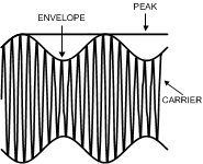
A peak detector is one of the simplest types of detectors. According to the naming, the peak detector stores the highest value arising in a certain time window. However, usually a peak detector is used with a relative long holding time when compared to the carrier frequency and a relative short holding time with respect to the envelope frequency. In this way a peak detector is used as AM demodulator or envelope tracker (Figure 42).
 Figure 42. Peak Detection vs. Envelope Tracking
A peak detector usually has a linear response. An example of this is a diode detector (Figure 43). The diode rectifies the RF input voltage and subsequently the RC filter determines the averaging (holding) time. The selection of the holding time configures the diode detector for its particular application. For envelope tracking a relatively small RC time constant is chosen, such that the output voltage tracks the envelope nicely. A configuration with a relatively large time constant can be used for supply regulation of the power amplifier (PA). Controlling the supply voltage of the PA can reduce power consumption significantly. The optimal mode of operation is to set the supply voltage such that it is just above the maximum output voltage of the PA. A diode detector with relative large RC time constant measures this maximum (peak) voltage.
 Figure 43. Diode Detector
Because peak detectors measure a peak voltage, their response is inherently depended on the signal shape or modulation form as discussed in the previous section. Knowledge about the signal shape is required to determine an RMS value. For complex systems having various modulation schemes, the amount of calibration and look-up tables can become unmanageable.
7.3.2.2 LOG Amp Detectors
LOG Amp detectors are widely used RF power detectors for GSM and the early W-CDMA systems. The transfer function of a LOG amp detector has a linear-in-dB response, which means that the output in volts changes linearly with the RF power in dBm. This is convenient because most communication standards specify transmit power levels in dBm as well. LOG amp detectors implement the logarithmic function by a piecewise linear approximation. Consequently, the LOG amp detector does not implement an exact power measurement, which implies a dependency on the signal shape. In systems using various modulation schemes calibration and lookup tables might be required.
7.3.2.3 RMS Detectors
An RMS detector has a response that is insensitive to the signal shape and modulation form. This is because its operation is based on exact determination of the average power, that is, it implements:

RMS detectors are in particular suited for the newer communication standards like W-CDMA and LTE that exhibit large peak-to-average ratios and different modulation schemes (signal shapes). This is a key advantage compared to other types of detectors in applications that employ signals with high peak-to-average power variations or different modulation schemes. For example, the RMS detector response to a 0-dBm modulated W-CDMA signal and a 0-dBm unmodulated carrier is essentially equal. This eliminates the need for long calibration procedures and large calibration tables in the baseband due to different applied modulation schemes.
7.3.3 LMH2110 RF Power Detector
For optimal performance of the LMH2110, the device must to be configured correctly in the application (see Functional Block Diagram).
For measuring the RMS (power) level of a signal, the time average of the squared signal needs to be measured as described in Accurate Power Measurement. This is implemented in the LMH2110 by means of a multiplier and a low-pass filter in a negative-feedback loop. A simplified block diagram of the LMH2110 is depicted in Functional Block Diagram. The core of the loop is a multiplier. The two inputs of the multiplier are fed by (i1, i2):
where
- iLF is a current depending on the DC output voltage of the RF detector, and
- iRF is a current depending on the RF input signal.
The output of the multiplier (iOUT) is the product of these two current and equals:

where
- I0 is a normalizing current.
By a low-pass filter at the output of the multiplier the DC term of this current is isolated and integrated. The input of the amplifier A acts as the nulling point of the negative feedback loop, yielding:

which implies that the average power content of the current related to the output voltage of the LMH2110 is made equal to the average power content of the current related to the RF input signal.
For a negative-feedback system, the transfer function is given by the inverse function of the feedback block. Therefore, to have a logarithmic transfer for this RF detector, the feedback network implements an exponential function resulting in an overall transfer function for the LMH2110 of:

where
- V0 and VX are normalizing voltages.
As a result of the feedback loop a square-root is also implemented, yielding the RMS function.
Given this architecture for the RF detector, the high-performance of the LMH2110 can be understood. In theory the accuracy of the logarithmic transfer is set by:
- The exponential feedback network, which basically needs to process a DC signal only.
- A high loop gain for the feedback loop, which is specified by the amplifier gain A.
The RMS functionality is inherent to the feedback loop and the use of a multiplier; thus, a very accurate LOG-RMS RF power detector is obtained.
To ensure a low dependency on the supply voltage, the internal detector circuitry is supplied via a low drop-out (LDO) regulator. This enables the usage of a wide range of supply voltage (2.7 V to 5 V) in combination with a low sensitivity of the output signal for the external supply voltage.
7.3.3.1 RF Input
Refer to Application With Resistive Divider for more details and applications.
7.3.3.2 Enable
To save power, the LMH2110 can be brought into a low-power shutdown mode by means of the enable pin (EN). The device is active for EN = HIGH (VEN>1.1 V) and in the low-power shutdown mode for EN = LOW
(VEN < 0.6 V). In this state the output of the LMH2110 is switched to a high impedance mode. This high impedance mode prevents the discharge of the optional low-pass filter which is good for the power efficiency. Using the shutdown function, care must be taken not to exceed the absolute maximum ratings. Because the device has an internal operating voltage of 2.5 V, the voltage level on the enable must not be higher than 3 V to prevent damage to the device. Also enable voltage levels lower than 400 mV below GND must be prevented. In both cases the ESD devices start to conduct when the enable voltage range is exceeded, and excessive current is drawn. A correct operation is not ensured then. The absolute maximum ratings are also exceeded when the enable (EN) is switched to HIGH (from shutdown to active mode) while the supply voltage is switched off. This situation must be prevented at all times. A possible solution to protect the device is to add a resistor of 1 kΩ in series with the enable input to limit the current.
7.3.3.3 Output
Refer to Application With Low-Pass Output Filter for Residual Ripple Reduction for more details and applications.
7.3.3.4 Supply
The LMH2110 has an internal LDO to handle supply voltages between 2.7 V to 5 V. This enables a direct connection to the battery in cell-phone applications. The high PSRR of the LMH2110 ensures that the performance is constant over its power supply range.
7.4 Device Functional Modes
To save power, the LMH2120 has an Enable/Disable feature that can bring the device in low-power shutdown mode. For implementation details, refer to Enable.