SNWS022D January   2010  – June 2015 LMH2110

PRODUCTION DATA.  

  1. Features
  2. Applications
  3. Description
  4. Revision History
  5. Pin Configuration and Functions
  6. Specifications
    1. 6.1 Absolute Maximum Ratings
    2. 6.2 ESD Ratings
    3. 6.3 Recommended Operating Conditions
    4. 6.4 Thermal Information
    5. 6.5 2.7-V and 4.5-V DC and AC Electrical Characteristics
    6. 6.6 Timing Requirements
    7. 6.7 Typical Characteristics
  7. Detailed Description
    1. 7.1 Overview
    2. 7.2 Functional Block Diagram
    3. 7.3 Feature Description
      1. 7.3.1 Accurate Power Measurement
      2. 7.3.2 Types of RF Detectors
        1. 7.3.2.1 Peak Detectors
        2. 7.3.2.2 LOG Amp Detectors
        3. 7.3.2.3 RMS Detectors
      3. 7.3.3 LMH2110 RF Power Detector
        1. 7.3.3.1 RF Input
        2. 7.3.3.2 Enable
        3. 7.3.3.3 Output
        4. 7.3.3.4 Supply
    4. 7.4 Device Functional Modes
  8. Application and Implementation
    1. 8.1 Application Information
    2. 8.2 Typical Applications
      1. 8.2.1 Application With Transmit Power Control
        1. 8.2.1.1 Design Requirements
        2. 8.2.1.2 Detailed Design Procedure
          1. 8.2.1.2.1 Specifying Detector Performance
            1. 8.2.1.2.1.1 Dynamic Range
            2. 8.2.1.2.1.2 Log Conformance Error
            3. 8.2.1.2.1.3 Variation Over Temperature Error
            4. 8.2.1.2.1.4 1-dB Step Error
            5. 8.2.1.2.1.5 10-dB Step Error
            6. 8.2.1.2.1.6 Variation Due to Modulation
        3. 8.2.1.3 Application Curves
      2. 8.2.2 Application With Resistive Divider
      3. 8.2.3 Application With Low-Pass Output Filter for Residual Ripple Reduction
  9. Power Supply Recommendations
  10. 10Layout
    1. 10.1 Layout Guidelines
    2. 10.2 Layout Example
  11. 11Device and Documentation Support
    1. 11.1 Community Resources
    2. 11.2 Trademarks
    3. 11.3 Electrostatic Discharge Caution
    4. 11.4 Glossary
  12. 12Mechanical, Packaging, and Orderable Information

Package Options

Mechanical Data (Package|Pins)
Thermal pad, mechanical data (Package|Pins)
Orderable Information

5 Pin Configuration and Functions

YFQ Package
6-Bump DSBGA
Top View
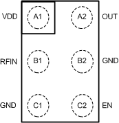
LMH2110 pins_snws022.gif

Pin Functions

PIN TYPE DESCRIPTION
NUMBER NAME
A1 VDD Power Supply Positive supply voltage.
A2 OUT Output Ground referenced detector output voltage.
B1 RFIN Analog Input RF input signal to the detector, internally terminated with 50 Ω.
B2 GND Power Supply Power Ground. May be left floating in case grounding is not feasible.
C1 GND Power Supply Power Ground.
C2 EN Logic Input The device is enabled for EN = High, and in shutdown mode for EN = Low. EN must be < 2.5 V to have low IEN. For EN > 2.5 V, IEN increases slightly, while device is still functional. Absolute maximum rating for EN = 3.6 V.