SBOS709A July 2016 – July 2016 LMH2832
PRODUCTION DATA.
- 1 Features
- 2 Applications
- 3 Description
- 4 Revision History
- 5 Device Comparison Table
- 6 Pin Configuration and Functions
- 7 Specifications
- 8 Parameter Measurement Information
- 9 Detailed Description
- 10Application and Implementation
- 11Power Supply Recommendations
- 12Layout
- 13Device and Documentation Support
- 14Mechanical, Packaging, and Orderable Information
Package Options
Mechanical Data (Package|Pins)
- RHA|40
Thermal pad, mechanical data (Package|Pins)
- RHA|40
Orderable Information
1 Features
- Dual-Channel, Individual SPI™-Controlled DVGA
- Single 5-V Supply
- –3-dB Bandwidth: 1.1 GHz (Max Gain)
- Flat Bandwidth Response: 300 MHz
- Channel-to-Channel Gain Matching: ±0.05 dB
- Channel-to-Channel Phase Matching: ±0.1°
- Gain:
- 30 dB to –9 dB
- 1-dB Steps ±0.2 dB
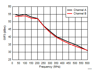
- Output Third-Order Intercept Point (OIP3):
- 43 dBm at 300 MHz
- 51 dBm at 200 MHz
- Noise Figure (NF):
- 6.5 dB (Max Gain) at 300 MHz, ZIN = 150 Ω
- Adjustable Power Consumption:
- 90 mA to 108 mA per Channel
- Power-Saving, Power-Down Feature:
- IQ < 4.5 mA per Channel
- Power-Down Pin and SPI Programmability
- Input Return Loss at 300 MHz:
- 17 dB (RS = 150 Ω)
2 Applications
- DOCSIS 3.1 CMTS Upstream Direct Sampling Receivers
- CATV Modem Signal Scaling
- Programmable Gain IF Amplifiers
- Generic RF, IF Gain Stages
- ADC Drivers
3 Description
The LMH2832 is a high-linearity, dual-channel, digital variable-gain amplifier (DVGA) for high-speed signal chain and data-acquisition systems. The LMH2832 is optimized to provide high bandwidth, low distortion, and low noise, thus making the device ideally suited as a dual, 14-bit, analog-to-digital converter (ADC) driver. The device consists of one fixed-gain block and one variable attenuator consisting of a total gain of 30 dB with a maximum attenuation of 39 dB. The gain range is from 30 dB to –9 dB in 1-dB gain steps with a gain accuracy of ±0.2 dB. The input impedance can be easily matched to 50-Ω or 75-Ω systems using a 1:3-Ω or 1:2-Ω ratio balun, respectively. The LMH2832 is designed to drive general-purpose ADCs and also meets the requirements for both data over cable service interface specification (DOCSIS) 3.0 32 quadrature amplitude modulation (QAM) carriers and DOCSIS 3.1 wideband orthogonal frequency-division multiplexing (OFDM) systems. With excellent NF (6.5 dB) and linearity, the LMH2832 is designed to perform to within DOCSIS specifications. The quiescent current in the power-down state is less than 5 mA per channel with the typical current consumption during operation at 105 mA per channel.
Device Information(1)
| PART NUMBER | PACKAGE | BODY SIZE (NOM) |
|---|---|---|
| LMH2832 | VQFN (40) | 6.00 mm × 6.00 mm |
- For all available packages, see the orderable addendum at the end of the data sheet.
Output Third-Order Intercept Point (OIP3) Performance
