SBOSAF0A april 2023 – august 2023 LMH32401-Q1
PRODUCTION DATA
- 1
- 1 Features
- 2 Applications
- 3 Description
- 4 Revision History
- 5 Pin Configuration and Functions
-
6 Specifications
- 6.1 Absolute Maximum Ratings
- 6.2 ESD Ratings
- 6.3 Recommended Operating Conditions
- 6.4 Thermal Information
- 6.5 Electrical Characteristics: Gain = 2 kΩ
- 6.6 Electrical Characteristics: Gain = 20 kΩ
- 6.7 Electrical Characteristics: Both Gains
- 6.8 Electrical Characteristics: Logic Threshold and Switching Characteristics
- 6.9 Typical Characteristics
- 7 Detailed Description
- 8 Application and Implementation
- 9 Device and Documentation Support
- 10Mechanical, Packaging, and Orderable Information
Package Options
Mechanical Data (Package|Pins)
- RGT|16
Thermal pad, mechanical data (Package|Pins)
- RGT|16
Orderable Information
8.2.3 Application Curves
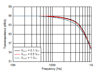
 Figure 8-4 Bandwidth vs Output Swing
(Gain = 2 kΩ)
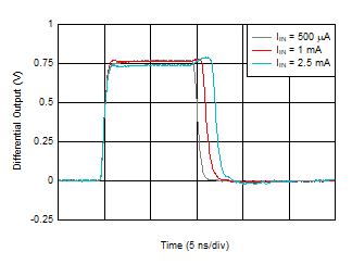
 Figure 8-6 Pulse Response vs Input Current
(Gain = 2 kΩ)
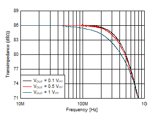
 Figure 8-5 Bandwidth vs Output Swing
(Gain = 20 kΩ)
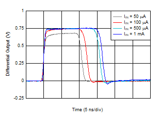
 Figure 8-7 Pulse Response vs Input Current
(Gain = 20 kΩ)