SBOS965D October 2019 – January 2023 LMH32401
PRODUCTION DATA
- 1 Features
- 2 Applications
- 3 Description
- 4 Revision History
- 5 Pin Configuration and Functions
-
6 Specifications
- 6.1 Absolute Maximum Ratings
- 6.2 ESD Ratings
- 6.3 Recommended Operating Conditions
- 6.4 Thermal Information
- 6.5 Electrical Characteristics: Gain = 2 kΩ
- 6.6 Electrical Characteristics: Gain = 20 kΩ
- 6.7 Electrical Characteristics: Both Gains
- 6.8 Electrical Characteristics: Logic Threshold and Switching Characteristics
- 6.9 Typical Characteristics
- 7 Detailed Description
- 8 Application and Implementation
- 9 Power Supply Recommendations
- 10Layout
- 11Device and Documentation Support
- 12Mechanical, Packaging, and Orderable Information
Package Options
Refer to the PDF data sheet for device specific package drawings
Mechanical Data (Package|Pins)
- RGT|16
- Y|0
Thermal pad, mechanical data (Package|Pins)
- RGT|16
Orderable Information
8.2 Typical Application
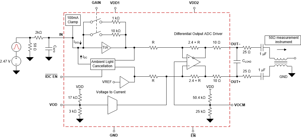
This section demonstrates the performance of the LMH32401 device when the input current flows into the IN pin. Figure 8-3 shows the circuit used to test the LMH32401 device with a voltage source. This configuration demonstrates the use case when the photodiode's anode is tied to the amplifier input and its cathode is tied to a positive voltage greater than 2.47 V.
 Figure 8-3 LMH32401 Test Circuit