SNOSAL8D April 2006 – September 2021 LMH6321
PRODUCTION DATA
- 1Features
- 2Applications
- 3Description
- 4Revision History
- 5Specifications
- 6Application Hints
- 7Device and Documentation Support
- 8Mechanical, Packaging, and Orderable Information
Package Options
Refer to the PDF data sheet for device specific package drawings
Mechanical Data (Package|Pins)
- KTW|7
- DDA|8
Thermal pad, mechanical data (Package|Pins)
Orderable Information
6.7 Output Current and Short Circuit Protection
The LMH6321 is designed to deliver a maximum continuous output current of 300 mA. However, the maximum available current, set by internal circuitry, is about 700 mA at room temperature. The output current is programmable up to 300 mA by a single external resistor and voltage source.
The LMH6321 is not designed to safely output 700 mA continuously and should not be used this way. However, the available maximum continuous current will likely be limited by the particular application and by the package type chosen, which together set the thermal conditions for the buffer (see Section 6.8) and could require less than 300 mA.
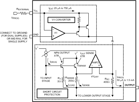
The programming of both the sourcing and sinking currents into the load is accomplished with a single resistor. Figure 6-3 shows a simplified diagram of the V to I converter and ISC protection circuitry that, together, perform this task.
Referring to Figure 6-3, the two simplified functional blocks, labeled V/I Converter and Short Circuit Protection, comprise the circuitry of the Current Limit Control.
The V/I converter consists of error amplifier A1 driving two PNP transistors in a Darlington configuration. The two input connections to this amplifier are VCL (inverting input) and GND (non-inverting input). If GND is connected to zero volts, then the high open loop gain of A1, as well as the feedback through the Darlington, will force CL, and thus one end REXT to be at zero volts also. Therefore, as shown in Equation 3 a voltage applied to the other end of REXT will force a current into this pin.
Through the VCL pin, IOUT is programmable from 10 mA to 300 mA by setting IEXT from 25 μA to 750 µA by means of a fixed REXT of 10 kΩ and making VPROG variable from 0.25 V to 7.5 V. Thus, an input voltage VPROG is converted to a current IEXT. This current is the output from the V/I converter. It is gained up by a factor of two and sent to the Short Circuit Protection block as IPROG. IPROG sets a voltage drop across RSC which is applied to the non-inverting input of error amp A2. The other input is across RSENSE. The current through RSENSE, and hence the voltage drop across it, is proportional to the load current, through the current sense transistor QSENSE. The output of A2 controls the drive (IDRIVE) to the base of the NPN output transistor, Q3 which is, proportional to the amount and polarity of the voltage differential (VDIFF) between AMP2 inputs, that is, how much the voltage across RSENSE is greater than or less than the voltage across RSC. This loop gains IEXT up by another 200, thus
Therefore, combining Equation 3 and Equation 4, and solving for REXT, we get
If the VCL pin is left open, the output short circuit current will default to about 700 mA. At elevated temperatures this current will decrease.
