SNOSAL8D April 2006 – September 2021 LMH6321
PRODUCTION DATA
- 1Features
- 2Applications
- 3Description
- 4Revision History
- 5Specifications
- 6Application Hints
- 7Device and Documentation Support
- 8Mechanical, Packaging, and Orderable Information
Package Options
Refer to the PDF data sheet for device specific package drawings
Mechanical Data (Package|Pins)
- KTW|7
- DDA|8
Thermal pad, mechanical data (Package|Pins)
Orderable Information
6.8.4 Example
Assume the following conditions:
- From Equation 7
- PD(MAX) = IS (2 V+) + V+2/4RL = (15 mA)(30 V) + 15 V2/200 Ω = 1.58 W
- From Equation 8
- TR(MAX) = 125°C - 85°C = 40°C
- From Equation 9
- θJA = 40°C/1.58 W = 25.3°C/W
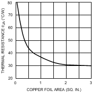
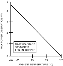
Examining Figure 6-4, we see that we cannot attain this low of a thermal resistance for one layer of 1 oz copper. It will be necessary to derate the part by decreasing either the ambient temperature or the power dissipation. Other solutions are to use two layers of 1 oz foil, or use 2 oz copper (see Table 6-1), or to provide forced air flow. One should allow about an extra 15% heat sinking capability for safety margin.
 Figure 6-4 Thermal Resistance (Typical)
for 7-L DDPAK Package Mounted on 1 oz. (0.036 mm) PC Board Foil
 Figure 6-5 Derating Curve for DDPAK
package. No Air Flow
Figure 6-5 Derating Curve for DDPAK
package. No Air Flow| Copper Area | θJA at 1.0W (°C/W) |
θJA at 2.0W (°C/W) |
|---|---|---|
| 1 Layer = 1”x2” cu Bottom | 62.4 | 54.7 |
| 2 Layer = 1”x2” cu Top and Bottom | 36.4 | 32.1 |
| 2 Layer = 2”x2” cu Top and Bottom | 23.5 | 22.0 |
| 2 Layer = 2”x4” cu Top and Bottom | 19.8 | 17.2 |
As seen in the previous example, buffer dissipation in DC circuit applications is easily computed. However, in AC circuits, signal wave shapes and the nature of the load (reactive, non-reactive) determine dissipation. Peak dissipation can be several times the average with reactive loads. It is particularly important to determine dissipation when driving large load capacitance.
A selection of thermal data for the SO PowerPAD package is shown in Table 6-2. The table summarizes θJA for both 0.5 watts and 0.75 watts. Note that the thermal resistance, for both the DDPAK and the SO PowerPAD package is lower for the higher power dissipation levels. This phenomenon is a result of the principle of Newtons Law of Cooling. Restated in term of heatsink cooling, this principle says that the rate of cooling and hence the thermal conduction, is proportional to the temperature difference between the junction and the outside environment (ambient). This difference increases with increasing power levels, thereby producing higher die temperatures with more rapid cooling.
| Copper Area/Vias | θJA at 0.5W (°C/W) |
θJA at 0.75W (°C/W) |
|---|---|---|
| 1 Layer = 0.05 sq. in. (Bottom) + 3 Via Pads | 141.4 | 138.2 |
| 1 Layer = 0.1 sq. in. (Bottom) + 3 Via Pads | 134.4 | 131.2 |
| 1 Layer = 0.25 sq. in. (Bottom) + 3 Via Pads | 115.4 | 113.9 |
| 1 Layer = 0.5 sq. in. (Bottom) + 3 Via Pads | 105.4 | 104.7 |
| 1 Layer = 1.0 sq. in. (Bottom) + 3 Via Pads | 100.5 | 100.2 |
| 2 Layer = 0.5 sq. in. (Top)/ 0.5 sq. in. (Bottom) + 33 Via Pads | 93.7 | 92.5 |
| 2 Layer = 1.0 sq. in. (Top)/ 1.0 sq. in. (Bottom) + 53 Via Pads | 82.7 | 82.2 |