SNOSAL8D April 2006 – September 2021 LMH6321
PRODUCTION DATA
- 1Features
- 2Applications
- 3Description
- 4Revision History
- 5Specifications
- 6Application Hints
- 7Device and Documentation Support
- 8Mechanical, Packaging, and Orderable Information
Package Options
Refer to the PDF data sheet for device specific package drawings
Mechanical Data (Package|Pins)
- KTW|7
- DDA|8
Thermal pad, mechanical data (Package|Pins)
Orderable Information
6.11 Slew Rate
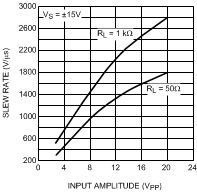
Slew rate is the rate of change of output voltage for large-signal step input changes. For resistive load, slew rate is limited by internal circuit capacitance and operating current (in general, the higher the operating current for a given internal capacitance, the faster is the slew rate). Figure 6-7 shows the slew capabilities of the LMH6321 under large signal input conditions, using a resistive load.
 Figure 6-7 Slew Rate vs. Peak-to-Peak Input Voltage
However, when driving capacitive loads, the slew rate may be limited by the available peak output current according to the following expression.
and rapidly changing output voltages will require large output load currents. For example if the part is required to slew at 1000 V/μs with a load capacitance of 1 nF the current demand from the LMH6321 would be 1A. Therefore, fast slew rate is incompatible with large CL. Also, since CL is in parallel with the load, the peak current available to the load decreases as CL increases.
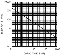
Figure 6-8 illustrates the effect of the load capacitance on slew rate. Slew rate tests are specified for resistive loads and/or very small capacitive loads, otherwise the slew rate test would be a measure of the available output current. For the highest slew rate, it is obvious that stray load capacitance should be minimized. Peak output current should be kept below 500 mA. This translates to a maximum stray capacitance of 500 pF for a slew rate of 1000 V/μs.
 Figure 6-8 Slew Rate vs. Load Capacitance