SNOSAL8D April 2006 – September 2021 LMH6321
PRODUCTION DATA
- 1Features
- 2Applications
- 3Description
- 4Revision History
- 5Specifications
- 6Application Hints
- 7Device and Documentation Support
- 8Mechanical, Packaging, and Orderable Information
Package Options
Refer to the PDF data sheet for device specific package drawings
Mechanical Data (Package|Pins)
- KTW|7
- DDA|8
Thermal pad, mechanical data (Package|Pins)
Orderable Information
3 Description
The LMH6321 is a high speed unity gain buffer that slews at 1800 V/µs and has a small signal bandwidth of 110 MHz while driving a 50 Ω load. It can drive ±300 mA continuously and will not oscillate while driving large capacitive loads.
The LMH6321 features an adjustable current limit. The current limit is continuously adjustable from 10 mA to 300 mA with a ±5 mA ±5% accuracy. The current limit is set by adjusting an external reference current with a resistor. The current can be easily and instantly adjusted, as needed by connecting the resistor to a DAC to form the reference current. The sourcing and sinking currents share the same current limit.
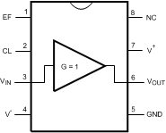
The LMH6321 is available in a space saving 8-pin SO PowerPAD or a 7-pin DDPAK power package. The SO PowerPAD™ package features an exposed pad on the bottom of the package to increase its heat sinking capability. The LMH6321 can be used within the feedback loop of an operational amplifier to boost the current output or as a stand alone buffer.
| PART NUMBER | PACKAGE(1) | BODY SIZE (NOM) |
|---|---|---|
| LMH6231 | SO PowerPAD (8) | 1.7 mm × 1.27 mm |
| DDPAK (7) | 4.65 mm × 1.27 mm |
 Figure 3-1 Connection Diagram: 8-Pin SO PowerPAD