SNOSB21E May 2008 – July 2024 LMH6518
PRODUCTION DATA
- 1
- 1 Features
- 2 Applications
- 3 Description
- 4 Pin Configuration and Functions
- 5 Specifications
- 6 Detailed Description
- 7 Application and Implementation
- 8 Device and Documentation Support
- 9 Revision History
- 10Mechanical, Packaging, and Orderable Information
Package Options
Refer to the PDF data sheet for device specific package drawings
Mechanical Data (Package|Pins)
- RGH|16
Thermal pad, mechanical data (Package|Pins)
- RGH|16
Orderable Information
7.2.2.1 Design Requirements
This circuit uses an N-Channel JFET (J10) in source-follower configuration to buffer the input signal with J8 acting as a constant current source. This buffer presents a fixed input impedance (1 MΩ || 10 pF) with a gain close to 1‑V/V.
The signal path is ac-coupled through C7 with dc (and low frequency) at LMH6518 +IN maintained through the action of U1. NPN transistor Q0 is an emitter follower which isolates the buffer from the load (LMH6518 input and board traces).
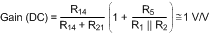
The undriven input of the LMH6518 (−IN) is biased to 2.5-V by R6, R9 voltage divider. The lower half of U1 inverts this voltage and the upper half of U1 compares this voltage to the combination of the driven output level at LMH6518 +IN and the scaled version of scope input at R14, R21 junction, and adjusts J10 Gate accordingly to set the LMH6518 +IN. This control loop has a frequency response that covers dc to a few Hz, limited by roll-off capacitor C3 and R15 combination (first order approximation). DC and low-frequency gain is given by Equation 18.
With the values in Figure 7-11 → R2 approximately 452 kΩ.
For a flat frequency response, the dc (low frequency) gain requires lowering to match the less-than-1 V/V ac (high frequency) path gain through the JFETs. This is done by increasing the value of R2.
Choose values of R15 and R11 so that the frequency response at J10 Gate (and consequently the output) remain flat when C7 starts to conduct as in Equation 19.

Offset correction is done by varying the voltage at R4, using a DAC or equivalent as shown, to shift the LMH6518 +IN voltage relative to −IN. The result is a circuit which shifts the ground referenced scope input to 2.5‑V (VCC / 2) CM with adjustable offset and without any JFET or BJT related offsets.
The front-end attenuator (not shown) lower leg resistance is increased for proper divider-ratio to account for the 1-MΩ shunt due to the series combination of R21 and R14. For example, a 10:1 front-end attenuator is formed by a series 900 kΩ and a shunt 111 kΩ for a scope BNC input impedance of 1 MΩ (= 900 K + (111 K || 1 M)).
Table 7-3 lists other possible JFET candidates that fall in the range of speed (ft) and low-noise requirement.
| COMPANY | PART NUMBER | VP (V) | Idss (mA) | gm (mS) | INPUT C (pF) | NOISE(1) (nV/RtHz) | BREAK DOWN (V) | CALCULATED ft (MHz) |
|---|---|---|---|---|---|---|---|---|
| Interfet | IF140 | –2.2 | 10 | 5.5 | 2.3 | 4 | –20 | 380 |
| Interfet | IF142 | –2.2 | 10 | 5.5 | 2.3 | 4 | –25 | 380 |
| Interfet | 2N5397/8 | –2.5 | 13 | 8 | 5 | 2.5 | –25 | 254 |
| Interfet | 2N5911/2 | –2.5 | 13 | 8 | 5 | 2.5 | — | 254 |
| Interfet | J308/9/10 | –2.3 | 21 | 17 | 5.8 | — | –25 | 466 |
| Philips | BF513 | –3 | 15 | 10 | 5 | — | — | 318 |
| Fairchild | MMBF5486 | –4 | 14 | 7 | 4 | 2.5 | –25 | 278 |
| Vishay Siliconix | SST441 | –3.5 | 13 | 6 | 3.5 | 4 | –35 | 272 |
The LNA noise can degrade the scope SNR if comparable to the input-referred noise of the LMH6518. LNA noise is influenced by the following operating conditions:
- JFET equivalent input noise
- BJT base current
Reducing either a or b above, or both, reduces noise. One way to reduce a is to increase R8 (currently set to 0 Ω). This reduces the noise impact of J8 but requires a JFET which has a higher Idss rating to maintain the operating current of J10, so that the J10 noise contribution is minimized. Reducing the BJT base current is accomplished with increasing R20 at the expenses of higher rise and fall times. A higher β also reduces the base current (keep in mind that β and ft at the operating collector current is what matters).
Figure 7-13 shows the impact of the JFET buffer noise on SNR, compared to SNR in Figure 7-3, assuming either 3‑nV/√Hz or 1.5-nV/√Hz buffer noise for comparison.