SNOSB21E May 2008 – July 2024 LMH6518
PRODUCTION DATA
- 1
- 1 Features
- 2 Applications
- 3 Description
- 4 Pin Configuration and Functions
- 5 Specifications
- 6 Detailed Description
- 7 Application and Implementation
- 8 Device and Documentation Support
- 9 Revision History
- 10Mechanical, Packaging, and Orderable Information
Package Options
Refer to the PDF data sheet for device specific package drawings
Mechanical Data (Package|Pins)
- RGH|16
Thermal pad, mechanical data (Package|Pins)
- RGH|16
Orderable Information
7.2.1.2.1 Settings and ADC SPI Code (ECM)
Covering the range from 1 mV/div to 10 V/div requires the following adjustment within the digital oscilloscope:
- Front-end attenuator
- LMH6518 preamp
- LMH6518 ladder attenuation
- ADC FS value (ECM)
The LMH6518 product folder contains a spreadsheet that helps calculate the front-end attenuator, LMH6518 preamp gain (HG or LG), ladder attenuation, and ADC FS setting based on the scope vertical scale (S in V/div).
The following step-by-step procedure explains the operations performed by the spreadsheet based on the scope vertical scale setting (S in V/div) and front-end attenuation A (from Table 7-1). A numerical example is also worked out for more clarification:
- Determine the required signal path gain, K, with
Equation 10: Equation 10.Assuming the full-scale signal occupies 95% of the 0.7 VPP FS for 5% overhead that occupies eight vertical scope divisions.
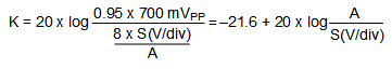
Required condition: −2.37 dB ≤ K ≤ 40.3 dB
Example: With S = 110 mV/div, Table 7-1 shows that A = 10 V/V in Equation 11.Equation 11.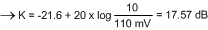
- Determine the LMH6518 gain, G:
G is the closest LMH6518 gain to the value of K where- G = (38.8 – 2n)dB; n = 0, 1, 2, …, 20
For this example, the closest G to K = 17.57 dB is 16.8 dB (with n = 11). The next LMH6518 gain, 18.8 dB (with n = 10) is incorrect as 16.8 is closer. If 18.8 dB were mistakenly selected, the ADC FS setting is out of range. Therefore, G = 16.8 dB
- Determine preamp (HG or LG) and ladder
attenuation:
- If G ≥ 18.8 dB → Preamp is HG and ladder attenuation = 38.8 – G
- If G < 18.8 dB → Preamp is LG and ladder attenuation = 18.8 – G
For this example, with G = 16.8 → Preamp LG and Ladder Attenuation = 2 dB (= 18.8 to 16.8).
- Determine the required
ADC FS voltage, FSE, with Equation 12: Equation 12.The 1.05 factor is to add 5% FS overhead margin to avoid ADC overdrive with Equation 13.
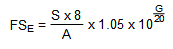 Equation 13.Required condition: 0.56 V ≤ FSE ≤ 0.84 V
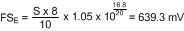
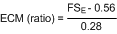
Recommend condition: 0.595 V ≤ FSE ≤ 0.805 V for optimum ADC FS - Determine the ADC ECM code ratio with Equation 14: Equation 14.
where
- 0.28 V = (0.84 – 0.56) V
- 0.56 V is the lower end of the ADC FS adjustability
For this example:
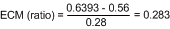
Required condition: 0 ≤ ECM (ratio) ≤ 1
- Determine the ECM binary code sent on ADC SPI
bus:
- Convert the ECM value represented by the ratio calculated previously, to binary:
- ECM (binary) =
DEC2BIN{ECM(ratio) × 511, 9}
where DEC2BIN is a spreadsheet function that converts the decimal ECM ratio, from step 5, multiplied by 511 distinct levels, into binary 9 bits.
Note: The web-based spreadsheet computes ECM without the use of DEC2BIN function to ease use by all spreadsheet users who do not have this function installed.For this example: ECM (binary) = DEC2BIN(0.283 × 511, 9) = 010010000. This number is sent to the ADC on the SPI bus to program the ADC to proper FS voltage.