SNOSAX9J April   2007  – April 2016 LMH6552

PRODUCTION DATA.  

  1. Features
  2. Applications
  3. Description
  4. Revision History
  5. Pin Configuration and Functions
  6. Specifications
    1. 6.1 Absolute Maximum Ratings
    2. 6.2 ESD Ratings
    3. 6.3 Recommended Operating Conditions
    4. 6.4 Thermal Information
    5. 6.5 Electrical Characteristics: ±5 V
    6. 6.6 Electrical Characteristics: ±2.5 V
    7. 6.7 Typical Characteristics V+ = +5 V, V− = −5 V
  7. Detailed Description
    1. 7.1 Overview
    2. 7.2 Functional Block Diagram
    3. 7.3 Feature Description
    4. 7.4 Device Functional Modes
  8. Application and Implementation
    1. 8.1 Application Information
    2. 8.2 Typical Applications
      1. 8.2.1 Typical Fully Differential Application
        1. 8.2.1.1 Design Requirements
        2. 8.2.1.2 Detailed Design Procedure
          1. 8.2.1.2.1 WSON Package
          2. 8.2.1.2.2 Fully Differential Operation
          3. 8.2.1.2.3 Driving Capacitive Loads
            1. 8.2.1.2.3.1 Balanced Cable Driver
        3. 8.2.1.3 Application Curves
      2. 8.2.2 Single-Ended Input to Differential Output Operation
      3. 8.2.3 Single Supply Operation
      4. 8.2.4 Split Supply Operation
      5. 8.2.5 Output Noise Performance and Measurement
      6. 8.2.6 Driving Analog to Digital Converters
  9. Power Supply Recommendations
    1. 9.1 Power Supply Bypassing
  10. 10Layout
    1. 10.1 Layout Guidelines
    2. 10.2 Layout Example
    3. 10.3 Thermal Considerations
    4. 10.4 Power Dissipation
    5. 10.5 ESD Protection
  11. 11Device and Documentation Support
    1. 11.1 Device Support
      1. 11.1.1 Third-Party Products Disclaimer
    2. 11.2 Documentation Support
      1. 11.2.1 Related Documentation
        1. 11.2.1.1 Evaluation Board
    3. 11.3 Community Resources
    4. 11.4 Trademarks
    5. 11.5 Electrostatic Discharge Caution
    6. 11.6 Glossary
  12. 12Mechanical, Packaging, and Orderable Information

Package Options

Mechanical Data (Package|Pins)
Thermal pad, mechanical data (Package|Pins)
Orderable Information

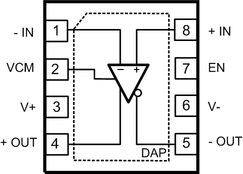
5 Pin Configuration and Functions

D Package
8 Pins
Top View
LMH6552 30003508.gif
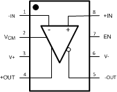
NGS Package
8 Pins
Top View
LMH6552 30003564.gif

Pin Functions

PIN DESCRIPTION
NAME NO.
EN 7 Enable
-IN 1 Negative Input
+IN 8 Positive Input
-OUT 5 Negative Output
+OUT 4 Positive Output
V- 6 Negative Supply
V+ 3 Positive Supply
VCM 2 Output Common Mode Control
DAP DAP Die Attach Pad (See Thermal Considerations for more information)