SNCS104D April 2005 – December 2014 LMH6570
PRODUCTION DATA.
- 1 Features
- 2 Applications
- 3 Description
- 4 Revision History
- 5 Pin Configuration and Functions
- 6 Specifications
- 7 Application and Implementation
- 8 Power Supply Recommendations
- 9 Layout
- 10Device and Documentation Support
- 11Mechanical, Packaging, and Orderable Information
Package Options
Mechanical Data (Package|Pins)
- D|8
Thermal pad, mechanical data (Package|Pins)
Orderable Information
1 Features
- 500 MHz, 500 mVPP, −3 dB Bandwidth, AV=2
- 400 MHz, 2VPP, −3 dB Bandwidth, AV=2
- 8 ns Channel Switching Time
- 70 dB Channel to Channel Isolation @ 10 MHz
- 0.02%, 0.05° Diff. Gain, Diff. Phase
- 0.1 dB Gain Flatness to 150 MHz
- 2200 V/μs Slew Rate
- Wide Supply Voltage Range: 6 V (±3 V) to 12 V (±6 V)
- −68 dB HD2 @ 5 MHz
- −84 dB HD3 @ 5 MHz
2 Applications
- Video Router
- Multi Input Video Monitor
- Instrumentation / Test Equipment
- Receiver IF Diversity Switch
- Multi Channel A/D Driver
- Picture in Picture Video Switch
3 Description
The LMH6570 is a high performance analog multiplexer optimized for professional grade video and other high fidelity, high bandwidth analog applications. The output amplifier selects one of two buffered input signals based on the state of the SEL pin. The LMH6570 provides a 400 MHz bandwidth at 2-VPP output signal levels. Multimedia and high definition television (HDTV) applications can benefit from the 0.1-dB bandwidth of 150 MHz and the 2200-V/μs slew rate of LMH6570.
The LMH6570 supports composite video applications with its 0.02% and 0.05° differential gain and phase errors for NTSC and PAL video signals while driving a single, back terminated 75-Ω load. An 80-mA linear output current is available for driving multiple video load applications.
The LMH6570 gain is set by external feedback and gain set resistors for maximum flexibility.
The LMH6570 is available in the 8-pin SOIC package.
Device Information(1)
| PART NUMBER | PACKAGE | BODY SIZE (NOM) |
|---|---|---|
| LMH6570 | SOIC (8) | 4.9 mm × 3.90 mm |
- For all available packages, see the orderable addendum at the end of the data sheet.
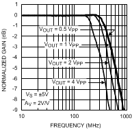
Frequency Response vs. VOUT
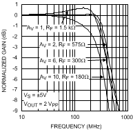
Frequency Response vs. Gain