SNOSB18I April 2010 – December 2014 LMH6629
PRODUCTION DATA.
- 1 Features
- 2 Applications
- 3 Description
- 4 Revision History
- 5 Pin Configuration and Functions
- 6 Specifications
-
7 Detailed Description
- 7.1 Overview
- 7.2 Functional Block Diagram
- 7.3
Feature Description
- 7.3.1 WSON-8 Control Pins and SOT-23-5 Comparison
- 7.3.2 Compensation
- 7.3.3 Cancellation of Offset Errors Due to Input Bias Currents
- 7.3.4 Total Input Noise vs. Source Resistance
- 7.3.5 Noise Figure
- 7.3.6 Single-Supply Operation
- 7.3.7 Low-Noise Transimpedance Amplifier
- 7.3.8 Low-Noise Integrator
- 7.3.9 High-Gain Sallen-Key Active Filters
- 7.4 Device Functional Modes
- 8 Application and Implementation
- 9 Power Supply Recommendations
- 10Layout
- 11Device and Documentation Support
- 12Mechanical, Packaging, and Orderable Information
Package Options
Mechanical Data (Package|Pins)
Thermal pad, mechanical data (Package|Pins)
Orderable Information
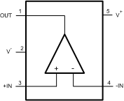
5 Pin Configuration and Functions
Package DBV
5-Pin
Top View

Package NGQ08A
8-Pin
Top View

Pin Functions
| NAME | NUMBER | I/O | DESCRIPTION | |
|---|---|---|---|---|
| DBV | NGQ08A | |||
| COMP | 6 | I | Compensation | |
| FB | 2 | I/O | Feedback | |
| -IN | 4 | 3 | I | Inverting input |
| +IN | 3 | 4 | I | Non-inverting input |
| OUT | 1 | 7 | O | Output |
| PD | 1 | I | Power Down | |
| V- | 2 | 5 | I | Negative supply |
| V+ | 5 | 8 | I | Positive supply |