LMH664x Low Power, 130 MHz, 75 mA Rail-to-Rail Output Amplifiers
1 Features
- −3 dB BW (AV = +1) 130 MHz
- Supply Voltage Range 2.7 V to 12.8 V
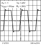
- Slew Rate, (AV = −1) 130V/µs(1)
- Supply Current (no load) 2.7 mA/amp
- Output Short Circuit Current +115 mA to 145 mA
- Linear Output Current ±75 mA
- Input Common Mode Volt. 0.5 V Beyond V−, 1 V from V+
- Output Voltage Swing 40 mV from Rails
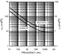
- Input Voltage Noise (100 kHz) 17nV/√Hz
- Input Current Noise (100 kHz) 0.9pA/√Hz
- THD (5MHz, RL = 2kΩ, VO = 2VPP, AV = +2) −62 dBc
- Settling Time 68 ns
- Fully Characterized for 3 V, 5 V, and ±5 V
- Overdrive Recovery 100 ns
- Output Short Circuit Protected(2)
- No Output Phase Reversal with CMVR Exceeded
(VS = ±5 V, TA = 25°C, RL = 2 kΩ, AV = +1. Typical Values Unless Specified).
2 Applications
- Active Filters
- CD/DVD ROM
- ADC Buffer Amp
- Portable Video
- Current Sense Buffer
3 Description
The LMH664X family true single supply voltage feedback amplifiers offer high speed (130 MHz), low distortion (−62 dBc), and exceptionally high output current (approximately 75 mA) at low cost and with reduced power consumption when compared against existing devices with similar performance.
Input common mode voltage range extends to 0.5 V below V− and 1 V from V+. Output voltage range extends to within 40 mV of either supply rail, allowing wide dynamic range especially desirable in low voltage applications. The output stage is capable of approximately 75 mA in order to drive heavy loads. Fast output Slew Rate (130 V/µs) ensures large peak-to-peak output swings can be maintained even at higher speeds, resulting in exceptional full power bandwidth of 40 MHz with a 3 V supply. These characteristics, along with low cost, are ideal features for a multitude of industrial and commercial applications.
Device Information(1)
| PART NUMBER | PACKAGE | BODY SIZE (NOM) |
|---|---|---|
| LMH6642 | SOT-23 (5) | 2.90 mm × 1.60 mm |
| SOIC (8) | 4.90 mm × 3.91 mm | |
| LMH6643 | SOIC (8) | 3.00 mm × 3.00 mm |
| VSSOP (8) | ||
| LMH6644 | SOIC (14) | 8.64 mm × 3.91 mm |
| TSSOP (14) | 5.00 mm × 4.40 mm |
- For all available packages, see the orderable addendum at the end of the datasheet.
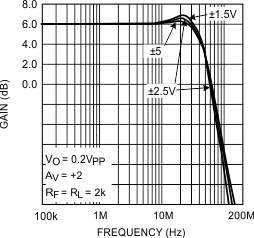
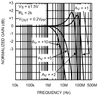
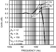
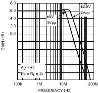
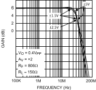
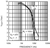
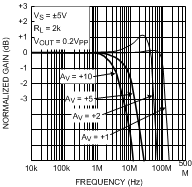
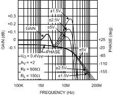
Closed Loop Gain vs. Frequency
for Various Supplies
4 Revision History
Changes from P Revision (March 2013) to Q Revision
- Added, revised, or updated the following sections: Device Information Table, Application and Implementation; Power Supply Recommendations; Device and Documentation Support; Mechanical, Packaging, and Ordering Information Go
- Changed "Junction Temperature Range" to "Operating Temperature Range"Go
- Deleted TJ = 25°C for Electrical Characteristics tables.Go
- Changed from "RL " to "Rf"Go
- Deleted TJ = 25°C for Typical Performance CharacteristicsGo
Changes from O Revision (March 2013) to P Revision
- Changed layout of National Data Sheet to TI formatGo
5 Description (continued)
Careful attention has been paid to ensure device stability under all operating voltages and modes. The result is a very well behaved frequency response characteristic (0.1dB gain flatness up the 12 MHz under 150 Ω load and AV = +2) with minimal peaking (typically 2dB maximum) for any gain setting and under both heavy and light loads. This along with fast settling time (68ns) and low distortion allows the device to operate well in an ADC buffer as well as high frequency filter applications.
This device family offers professional quality video performance with low DG (0.01%) and DP (0.01°) characteristics. Differential Gain and Differential Phase characteristics are also well maintained under heavy loads (150 Ω) and throughout the output voltage range. The LMH664X family is offered in single (LMH6642), dual (LMH6643), and quad (LMH6644) options.
6 Pin Configuration and Functions


Pin Functions
| PIN | I/O | DESCRIPTION | ||||
|---|---|---|---|---|---|---|
| NAME | LMH6642 | LMH6643 | LMH6644 | |||
| DBV05A | D08A | DGK08A | D14A and PW14A | |||
| -IN | 4 | 2 | I | Inverting Input | ||
| +IN | 3 | 3 | I | Non-inverting Input | ||
| -IN A | 2 | 2 | I | ChA Inverting Input | ||
| +IN A | 3 | 3 | I | ChA Non-inverting Input | ||
| -IN B | 6 | 6 | I | ChB Inverting Input | ||
| +IN B | 5 | 5 | I | ChB Non-inverting Input | ||
| -IN C | 9 | I | ChC Inverting Input | |||
| +IN C | 10 | I | ChC Non-inverting Input | |||
| -IN D | 13 | I | ChD Inverting Input | |||
| +IN D | 12 | I | ChD Non-inverting Input | |||
| N/C | 1,5,8 | –– | No connection | |||
| OUT A | 1 | 1 | O | ChA Output | ||
| OUT B | 7 | 7 | O | ChB Output | ||
| OUT C | 8 | O | ChC Output | |||
| OUT D | 14 | O | ChD Output | |||
| OUTPUT | 1 | 6 | O | Output | ||
| V- | 2 | 4 | 4 | 11 | I | Negative Supply |
| V+ | 5 | 7 | 8 | 4 | I | Positive Supply |
7 Specifications
7.1 Absolute Maximum Ratings(1)(2)
over operating free-air temperature range (unless otherwise noted)| MIN | MAX | UNIT | ||
|---|---|---|---|---|
| VIN Differential | ±2.5 | V | ||
| Output Short Circuit Duration | See (4) and (6) | |||
| Supply Voltage (V+ - V−) | 13.5 | V | ||
| Voltage at Input/Output pins | V+ +0.8 V− −0.8 |
V | ||
| Input Current | ±10 | mA | ||
| Junction Temperature(5) | +150 | °C | ||
| Soldering Information | Infrared or Convection Reflow (20 sec) | 235 | °C | |
| Wave Soldering Lead Temp.(10 sec) | 260 | °C | ||
7.2 Handling Ratings
| MIN | MAX | UNIT | |||
|---|---|---|---|---|---|
| Tstg | Storage temperature range | −65 | +150 | °C | |
| V(ESD) | Electrostatic discharge(3) | Human body model (HBM), per ANSI/ESDA/JEDEC JS-001, all pins(1) | 2000 | V | |
| Machine model (MM)(3) | 200 | ||||
| Charged device model (CDM), per JEDEC specification JESD22-C101, all pins(2) | 1000 | ||||
7.3 Recommended Operating Conditions(1)
over operating free-air temperature range (unless otherwise noted)| MIN | MAX | UNIT | ||
|---|---|---|---|---|
| Supply Voltage (V+ – V−) | 2.7 | 12.8 | V | |
| Operating Temperature Range(2) | −40 | +85 | °C | |
7.4 Thermal Information
| THERMAL METRIC(1) | LMH6642 | LMH6643 | LMH6644 | UNIT | |||
|---|---|---|---|---|---|---|---|
| DBV05A | D08A | DGK08A | D14A | PW14A | |||
| 5 PINS | 8 PINS | 8 PINS | 14 PINS | 14 PINS | |||
| RθJA | Junction-to-ambient Thermal Resistance(2) | 265 | 190 | 235 | 145 | 155 | °C/W |
7.5 3V Electrical Characteristics
Unless otherwise specified, all limits ensured for V+ = 3V, V− = 0V, VCM = VO = V+/2, VID (input differential voltage) as noted (where applicable) and RL = 2kΩ to V+/2.| PARAMETER | TEST CONDITIONS | AT TEMPERATURE EXTREMES |
V+ = 3V, V− = 0V, VCM = VO = V+/2, VID RL = 2 kΩ to V+/2 |
UNIT | |||||
|---|---|---|---|---|---|---|---|---|---|
| MIN | TYP | MAX | MIN(1) | TYP(2) | MAX(1) | ||||
| BW | −3dB BW | AV = +1, VOUT = 200mVPP | 80 | 115 | MHz | ||||
| AV = +2, −1, VOUT = 200mVPP | 46 | ||||||||
| BW0.1dB | 0.1dB Gain Flatness | AV = +2, RL = 150Ω to V+/2, Rf = 402Ω, VOUT = 200mVPP |
19 | MHz | |||||
| PBW | Full Power Bandwidth | AV = +1, −1dB, VOUT = 1VPP | 40 | MHz | |||||
| en | Input-Referred Voltage Noise | f = 100kHz | 17 | nV/√Hz | |||||
| f = 1kHz | 48 | ||||||||
| in | Input-Referred Current Noise | f = 100kHz | 0.90 | pA/√Hz | |||||
| f = 1kHz | 3.3 | ||||||||
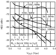
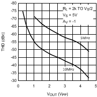
| THD | Total Harmonic Distortion | f = 5MHz, VO = 2VPP, AV = −1, RL = 100Ω to V+/2 |
−48 | dBc | |||||
| DG | Differential Gain | VCM = 1V, NTSC, AV = +2 RL =150Ω to V+/2 |
0.17% | ||||||
| RL =1kΩ to V+/2 | 0.03% | ||||||||
| DP | Differential Phase | VCM = 1V, NTSC, AV = +2 RL =150Ω to V+/2 |
0.05 | deg | |||||
| RL =1kΩ to V+/2 | 0.03 | ||||||||
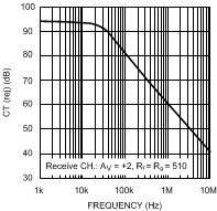
| CT Rej. | Cross-Talk Rejection | f = 5MHz, Receiver: Rf = Rg = 510Ω, AV = +2 |
47 | dB | |||||
| TS | Settling Time | VO = 2VPP, ±0.1%, 8pF Load, VS = 5V |
68 | ns | |||||
| SR | Slew Rate (3) | AV = −1, VI = 2VPP | 90 | 120 | V/µs | ||||
| VOS | Input Offset Voltage | For LMH6642 and LMH6644 | ±7 | ±1 | ±5 | mV | |||
| For LMH6643 | ±7 | ±1 | ±3.4 | ||||||
| TC VOS | Input Offset Average Drift | See (4) | ±5 | µV/°C | |||||
| IB | Input Bias Current | See (5) | −3.25 | −1.50 | −2.60 | µA | |||
| IOS | Input Offset Current | 1000 | 20 | 800 | nA | ||||
| RIN | Common Mode Input Resistance | 3 | MΩ | ||||||
| CIN | Common Mode Input Capacitance | 2 | pF | ||||||
| CMVR | Input Common-Mode Voltage Range | CMRR ≥ 50dB | −0.1 | −0.5 | −0.2 | V | |||
| 1.6 | 1.8 | 2.0 | |||||||
| CMRR | Common Mode Rejection Ratio | VCM Stepped from 0V to 1.5V | 72 | 95 | dB | ||||
| AVOL | Large Signal Voltage Gain | VO = 0.5V to 2.5V RL = 2kΩ to V+/2 |
75 | 80 | 96 | dB | |||
| VO = 0.5V to 2.5V RL = 150Ω to V+/2 |
70 | 74 | 82 | ||||||
| VO | Output Swing High |
RL = 2kΩ to V+/2, VID = 200mV | 2.90 | 2.98 | V | ||||
| RL = 150Ω to V+/2, VID = 200mV | 2.80 | 2.93 | |||||||
| Output Swing Low |
RL = 2kΩ to V+/2, VID = −200mV | 25 | 75 | mV | |||||
| RL = 150Ω to V+/2, VID = −200mV | 75 | 150 | |||||||
| ISC | Output Short Circuit Current | Sourcing to V+/2 VID = 200mV (6) |
35 | 50 | 95 | mA | |||
| Sinking to V+/2 VID = −200mV (6) |
40 | 55 | 110 | ||||||
| IOUT | Output Current | VOUT = 0.5V from either supply | ±65 | mA | |||||
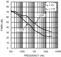
| +PSRR | Positive Power Supply Rejection Ratio | V+ = 3.0V to 3.5V, VCM = 1.5V | 75 | 85 | dB | ||||
| IS | Supply Current (per channel) | No Load | 4.50 | 2.70 | 4.00 | mA | |||
7.6 5V Electrical Characteristics
Unless otherwise specified, all limits ensured for V+ = 5V, V− = 0V, VCM = VO = V+/2, VID (input differential voltage) as noted (where applicable) and RL = 2kΩ to V+/2.| PARAMETER | TEST CONDITIONS | AT TEMPERATURE EXTREMES | V+ = 5V, V− = 0V, VCM = VO = V+/2, VID RL = 2kΩ to V+/2 |
UNIT | |||||
|---|---|---|---|---|---|---|---|---|---|
| MIN | TYP | MAX | MIN(1) | TYP(2) | MAX(1) | ||||
| BW | −3dB BW | AV = +1, VOUT = 200mVPP | 90 | 120 | MHz | ||||
| AV = +2, −1, VOUT = 200mVPP | 46 | ||||||||
| BW0.1dB | 0.1dB Gain Flatness | AV = +2, RL = 150Ω to V+/2, Rf = 402Ω, VOUT = 200mVPP |
15 | MHz | |||||
| PBW | Full Power Bandwidth | AV = +1, −1dB, VOUT = 2VPP | 22 | MHz | |||||
| en | Input-Referred Voltage Noise | f = 100kHz | 17 | nV/√Hz | |||||
| f = 1kHz | 48 | ||||||||
| in | Input-Referred Current Noise | f = 100kHz | 0.90 | pA/√Hz | |||||
| f = 1kHz | 3.3 | ||||||||
| THD | Total Harmonic Distortion | f = 5MHz, VO = 2VPP, AV = +2 | −60 | dBc | |||||
| DG | Differential Gain | NTSC, AV = +2 RL =150Ω to V+/2 |
0.16% | ||||||
| RL = 1kΩ to V+/2 | 0.05% | ||||||||
| DP | Differential Phase | NTSC, AV = +2 RL = 150Ω to V+/2 |
0.05 | deg | |||||
| RL = 1kΩ to V+/2 | 0.01 | ||||||||
| CT Rej. | Cross-Talk Rejection | f = 5MHz, Receiver: Rf = Rg = 510Ω, AV = +2 |
47 | dB | |||||
| TS | Settling Time | VO = 2VPP, ±0.1%, 8pF Load | 68 | ns | |||||
| SR | Slew Rate (3) | AV = −1, VI = 2VPP | 95 | 125 | V/µs | ||||
| VOS | Input Offset Voltage | For LMH6642 and LMH6644 | ±7 | ±1 | ±5 | mV | |||
| For LMH6643 | ±7 | ±1 | ±3.4 | ||||||
| TC VOS | Input Offset Average Drift | See (4) | ±5 | µV/°C | |||||
| IB | Input Bias Current | See (5) | −3.25 | −1.70 | −2.60 | µA | |||
| IOS | Input Offset Current | 1000 | 20 | 800 | nA | ||||
| RIN | Common Mode Input Resistance | 3 | MΩ | ||||||
| CIN | Common Mode Input Capacitance | 2 | pF | ||||||
| CMVR | Input Common-Mode Voltage Range | CMRR ≥ 50dB | −0.1 | −0.5 | −0.2 | V | |||
| 3.6 | 3.8 | 4.0 | |||||||
| CMRR | Common Mode Rejection Ratio | VCM Stepped from 0V to 3.5V | 72 | 95 | dB | ||||
| AVOL | Large Signal Voltage Gain | VO = 0.5V to 4.50V RL = 2kΩ to V+/2 |
82 | 86 | 98 | dB | |||
| VO = 0.5V to 4.25V RL = 150Ω to V+/2 |
72 | 76 | 82 | ||||||
| VO | Output Swing High |
RL = 2kΩ to V+/2, VID = 200mV | 4.90 | 4.98 | V | ||||
| RL = 150Ω to V+/2, VID = 200mV | 4.65 | 4.90 | |||||||
| Output Swing Low |
RL = 2kΩ to V+/2, VID = −200mV | 25 | 100 | mV | |||||
| RL = 150Ω to V+/2, VID = −200mV | 100 | 150 | |||||||
| ISC | Output Short Circuit Current | Sourcing to V+/2 VID = 200mV (6)(7) |
40 | 55 | 115 | mA | |||
| Sinking to V+/2 VID = −200mV (6)(7) |
55 | 70 | 140 | ||||||
| IOUT | Output Current | VO = 0.5V from either supply | ±70 | mA | |||||
| +PSRR | Positive Power Supply Rejection Ratio | V+ = 4.0V to 6V | 79 | 90 | dB | ||||
| IS | Supply Current (per channel) | No Load | 5.00 | 2.70 | 4.25 | mA | |||
7.7 ±5V Electrical Characteristics
Unless otherwise specified, all limits ensured for V+ = 5V, V− = −5V, VCM = VO = 0V, VID (input differential voltage) as noted (where applicable) and RL = 2kΩ to ground.| PARAMETER | TEST CONDITIONS | AT TEMPERATURE EXTREMES | V+ = 5V, V− = −5V, VCM = VO = 0V, VID |
UNIT | |||||
|---|---|---|---|---|---|---|---|---|---|
| MIN | TYP | MAX | MIN(2) | TYP(1) | MAX(2) | ||||
| BW | −3dB BW | AV = +1, VOUT = 200mVPP | 95 | 130 | MHz | ||||
| AV = +2, −1, VOUT = 200mVPP | 46 | ||||||||
| BW0.1dB | 0.1dB Gain Flatness | AV = +2, RL = 150Ω to V+/2, Rf = 806Ω, VOUT = 200mVPP |
12 | MHz | |||||
| PBW | Full Power Bandwidth | AV = +1, −1dB, VOUT = 2VPP | 24 | MHz | |||||
| en | Input-Referred Voltage Noise | f = 100kHz | 17 | nV/√Hz | |||||
| f = 1kHz | 48 | ||||||||
| in | Input-Referred Current Noise | f = 100kHz | 0.90 | pA/√Hz | |||||
| f = 1kHz | 3.3 | ||||||||
| THD | Total Harmonic Distortion | f = 5MHz, VO = 2VPP, AV = +2 | −62 | dBc | |||||
| DG | Differential Gain | NTSC, AV = +2 RL = 150Ω to V+/2 |
0.15% | ||||||
| RL = 1kΩ to V+/2 | 0.01% | ||||||||
| DP | Differential Phase | NTSC, AV = +2 RL = 150Ω to V+/2 |
0.04 | deg | |||||
| RL = 1kΩ to V+/2 | 0.01 | ||||||||
| CT Rej. | Cross-Talk Rejection | f = 5MHz, Receiver: Rf = Rg = 510Ω, AV = +2 |
47 | dB | |||||
| TS | Settling Time | VO = 2VPP, ±0.1%, 8pF Load, VS = 5V |
68 | ns | |||||
| SR | Slew Rate (4) | AV = −1, VI = 2VPP | 100 | 135 | V/µs | ||||
| VOS | Input Offset Voltage | For LMH6642 and LMH6644 | ±7 | ±1 | ±5 | mV | |||
| For LMH6643 | ±7 | ±1 | ±3.4 | ||||||
| TC VOS | Input Offset Average Drift | See (7) | ±5 | µV/°C | |||||
| IB | Input Bias Current | See (3) | −3.25 | −1.60 | −2.60 | µA | |||
| IOS | Input Offset Current | 1000 | 20 | 800 | nA | ||||
| RIN | Common Mode Input Resistance | 3 | MΩ | ||||||
| CIN | Common Mode Input Capacitance | 2 | pF | ||||||
| CMVR | Input Common-Mode Voltage Range | CMRR ≥ 50dB | −5.1 | −5.5 | −5.2 | V | |||
| 3.6 | 3.8 | 4.0 | |||||||
| CMRR | Common Mode Rejection Ratio | VCM Stepped from −5V to 3.5V | 74 | 95 | dB | ||||
| AVOL | Large Signal Voltage Gain | VO = −4.5V to 4.5V, RL = 2kΩ |
84 | 88 | 96 | dB | |||
| VO = −4.0V to 4.0V, RL = 150Ω |
74 | 78 | 82 | ||||||
| VO | Output Swing High |
RL = 2kΩ, VID = 200mV | 4.90 | 4.96 | V | ||||
| RL = 150Ω, VID = 200mV | 4.65 | 4.80 | |||||||
| Output Swing Low |
RL = 2kΩ, VID = −200mV | −4.96 | −4.90 | V | |||||
| RL = 150Ω, VID = −200mV | −4.80 | −4.65 | |||||||
| ISC | Output Short Circuit Current | Sourcing to Ground VID = 200mV (5)(6) |
35 | 60 | 115 | mA | |||
| Sinking to Ground VID = −200mV (5)(6) |
65 | 85 | 145 | ||||||
| IOUT | Output Current | VO = 0.5V from either supply | ±75 | mA | |||||
| PSRR | Power Supply Rejection Ratio | (V+, V−) = (4.5V, −4.5V) to (5.5V, −5.5V) | 78 | 90 | dB | ||||
| IS | Supply Current (per channel) | No Load | 5.50 | 2.70 | 4.50 | mA | |||
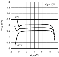
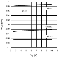
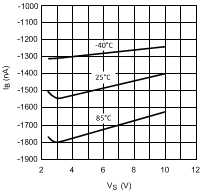
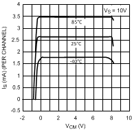
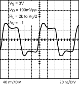
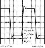
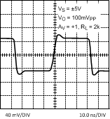
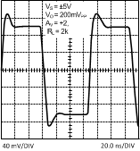
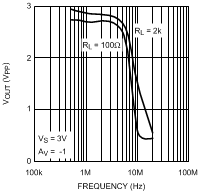
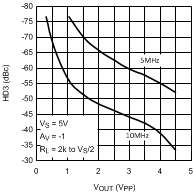
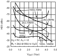
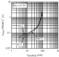
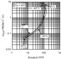
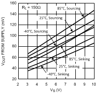
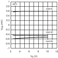
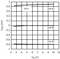
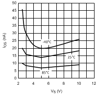
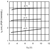
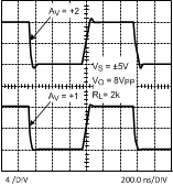
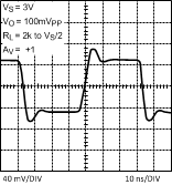
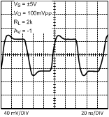
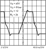
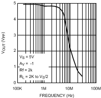
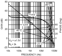
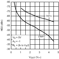
7.8 Typical Performance Characteristics
V+ = +5, V− = −5V, RF = RL = 2 kΩ. Unless otherwise specified.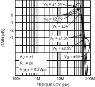
for Various Supplies
for Various Gain
for Various Supplies
for Various Supplies
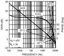
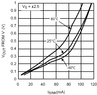
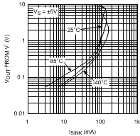
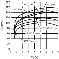
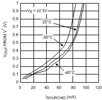
for Various Temperature
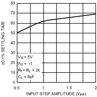
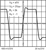
(Output Slew and Settle Time)
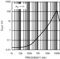
vs. Frequency AV = +1
for Various Gain
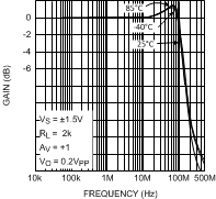
for Various Temperature
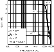
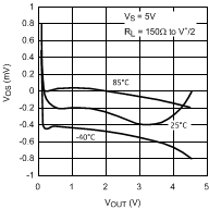
for Various Temperature
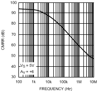
for Various Supplies
for Various Supplies
for Various Temperature
(Output to Output)