SBOS996C May 2020 – May 2021 LMH9235
PRODUCTION DATA
- 1 Features
- 2 Applications
- 3 Description
- 4 Revision History
- 5 Pin Configuration and Functions
- 6 Specifications
- 7 Detailed Description
- 8 Application and Implementation
- 9 Power Supply Recommendations
- 10Layout
- 11Device and Documentation Support
- 12Mechanical, Packaging, and Orderable Information
Package Options
Mechanical Data (Package|Pins)
- RRL|12
Thermal pad, mechanical data (Package|Pins)
Orderable Information
7.3 Feature Description
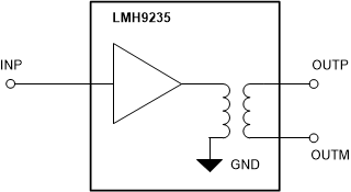
The LMH9235 device is single-ended to differential RF amplifier for narrow band active balun implementation. The device integrates the functionality of a single-ended RF amplifier and passive balun in traditional receive applications achieving small form factor with comparable linearity and noise performance, as shown in Figure 7-2.
The active balun implementation coupled with higher operating temperature of 105°C allows for more robust receiver system implementation compared to passive balun that is prone to reliability failures at high temperatures. The high temperature operation is achieved by the on-chip active bias circuitry which maintains device performance over a wide temperature and supply voltage range.
 Figure 7-2 Single-Ended Input to Differential Output, Active Balun Implementation