SNAS579G March   2012  – December 2014 LMK00105

PRODUCTION DATA.  

  1. Features
  2. Applications
  3. Description
    1.     Device Images
      1.      Functional Block Diagram
  4. Revision History
  5. Pin Configuration and Diagrams
    1.     Pin Functions
  6. Specifications
    1. 6.1 Absolute Maximum Ratings
    2. 6.2 ESD Ratings
    3. 6.3 Recommended Operating Conditions
    4. 6.4 Thermal Information
    5. 6.5 Electrical Characteristics
    6. 6.6 Typical Characteristics
  7. Detailed Description
    1. 7.1 Overview
    2. 7.2 Functional Block Diagram
    3. 7.3 Feature Description
      1. 7.3.1 Vdd and Vddo Power Supplies
      2. 7.3.2 Clock Input
        1. 7.3.2.1 Selection of Clock Input
          1. 7.3.2.1.1 CLKin/CLKin* Pins
          2. 7.3.2.1.2 OSCin/OSCout Pins
      3. 7.3.3 Clock Outputs
        1. 7.3.3.1 Output Enable Pin
        2. 7.3.3.2 Using Less than Five Outputs
    4. 7.4 Device Functional Modes
  8. Application and Implementation
    1. 8.1 Application Information
      1. 8.1.1 Clock Inputs
      2. 8.1.2 Clock Outputs
    2. 8.2 Typical Applications
      1. 8.2.1 Typical Application Block Diagram
        1. 8.2.1.1 Design Requirements
        2. 8.2.1.2 Detailed Design Procedure
        3. 8.2.1.3 Application Curves
      2. 8.2.2 Crystal Interface
        1. 8.2.2.1 Design Requirements
        2. 8.2.2.2 Detailed Design Procedure
        3. 8.2.2.3 Application Curves
  9. Power Supply Recommendations
    1. 9.1 Power Supply Filtering
    2. 9.2 Power Supply Ripple Rejection
    3. 9.3 Power Supply Bypassing
  10. 10Layout
    1. 10.1 Layout Guidelines
      1. 10.1.1 Ground Planes
      2. 10.1.2 Power Supply Pins
      3. 10.1.3 Differential Input Termination
      4. 10.1.4 Output Termination
    2. 10.2 Layout Example
    3. 10.3 Thermal Management
  11. 11Device and Documentation Support
    1. 11.1 Documentation Support
      1. 11.1.1 Differential Voltage Measurement Terminology
    2. 11.2 Trademarks
    3. 11.3 Electrostatic Discharge Caution
    4. 11.4 Glossary
  12. 12Mechanical, Packaging, and Orderable Information

Package Options

Refer to the PDF data sheet for device specific package drawings

Mechanical Data (Package|Pins)
  • RTW|24
Thermal pad, mechanical data (Package|Pins)
Orderable Information

Clock Outputs

The LMK00105 LVCMOS driver output impedance (Ro) is nominally 50 ohms and well-matched to drive a 50 ohm transmission line (Zo), as shown as below. If driving a transmission line with higher characteristic impedance than 50 ohms, a series resistor (Rs) should be placed near the driver to provide source termination, where Rs = Zo – Ro.

The LMK00105 has two output banks, Bank A and Bank B, which are separately powered by independent Vddo supply pins. The Vddo supply pins for Bank A and Bank B are not connected together internally, and may be supplied with different voltages. This allows the LMK00105 outputs to easily interface to multiple receivers with different input threshold or input supply voltage (Vddi) requirements without the need for additional voltage divider networks.
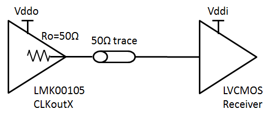
LMK00105 clockinput_snas579.pngFigure 9. LMK00105 Output Termination