SNAS579G March 2012 – December 2014 LMK00105
PRODUCTION DATA.
- 1 Features
- 2 Applications
- 3 Description
- 4 Revision History
- 5 Pin Configuration and Diagrams
- 6 Specifications
- 7 Detailed Description
- 8 Application and Implementation
- 9 Power Supply Recommendations
- 10Layout
- 11Device and Documentation Support
- 12Mechanical, Packaging, and Orderable Information
Package Options
Refer to the PDF data sheet for device specific package drawings
Mechanical Data (Package|Pins)
- RTW|24
Thermal pad, mechanical data (Package|Pins)
Orderable Information
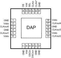
5 Pin Configuration and Diagrams
24-Pin
WQFN Package
Top View

Pin Functions
| PIN | TYPE | DESCRIPTION | |
|---|---|---|---|
| NAME | NO | ||
| DAP | DAP | — | The DAP should be grounded |
| Vddo | 2, 6 | Power | Power Supply for Bank A (CLKout0 and CLKout 1) CLKout pins. |
| CLKout0 | 3 | Output | LVCMOS Output |
| GND | 1,4,7,11,
12, 16,19 |
GND | Ground |
| CLKout1 | 5 | Output | LVCMOS Output |
| Vdd | 8,23 | Power | Supply for operating core and input buffer |
| OSCin | 9 | Input | Input for Crystal |
| OSCout | 10 | Output | Output for Crystal |
| CLKout2 | 13 | Output | LVCMOS Output |
| Vddo | 14,18 | Power | Power Supply for Bank B (CLKout2 to CLKout 4) CLKout pins |
| CLKout3 | 15 | Output | LVCMOS Output |
| CLKout4 | 17 | Output | LVCMOS Output |
| CLKin* | 20 | Input | Complementary input pin |
| CLKin | 21 | Input | Input Pin |
| SEL | 22 | Input | Input Clock Selection. This pin has an internal pulldown resistor.(1) |
| OE | 24 | Input | Output Enable. This pin has an internal pulldown resistor.(1) |
(1) CMOS control input with internal pulldown resistor.