SNAS522K September   2011  – December 2023 LMK03806

PRODUCTION DATA  

  1.   1
  2. Features
  3. Applications
  4. Description
  5. Pin Configuration and Functions
  6. Specifications
    1. 5.1 Absolute Maximum Ratings
    2. 5.2 ESD Ratings
    3. 5.3 Recommended Operating Conditions
    4. 5.4 Thermal Information
    5. 5.5 Electrical Characteristics
    6. 5.6 Timing Requirements
    7. 5.7 Typical Characteristics
  7. Parameter Measurement Information
    1. 6.1 Differential Voltage Measurement Terminology
  8. Detailed Description
    1. 7.1 Overview
    2. 7.2 Functional Block Diagrams
    3. 7.3 Features Description
      1. 7.3.1 Serial MICROWIRE Timing Diagram and Terminology
      2. 7.3.2 Crystal Support With Buffered Outputs
      3. 7.3.3 Integrated Loop Filter Poles
      4. 7.3.4 Integrated VCO
      5. 7.3.5 Clock Distribution
        1. 7.3.5.1 CLKout DIvider
        2. 7.3.5.2 Programmable Output Type
        3. 7.3.5.3 Clock Output Synchronization
      6. 7.3.6 Default Start-Up Clocks
    4. 7.4 Device Functional Modes
    5. 7.5 Programming
      1. 7.5.1 General Information
        1. 7.5.1.1 Special Programming Case for R0 to R5 for CLKoutX_Y_DIV > 25
        2. 7.5.1.2 Recommended Initial Programming Sequence
        3. 7.5.1.3 READBACK
          1. 7.5.1.3.1 Readback Example
  9. Application and Implementation
    1. 8.1 Application Information
      1. 8.1.1 Crystal Interface
      2. 8.1.2 Driving OSCin Pins With a Single-Ended Source
      3. 8.1.3 Driving OSCin Pins With a Differential Source
      4. 8.1.4 Frequency Planning With the LMK03806
      5. 8.1.5 Configuring the PLL
        1. 8.1.5.1 Example PLL Configuration
      6. 8.1.6 Digital Lock Detect
    2. 8.2 Typical Application
      1. 8.2.1 Design Requirements
      2. 8.2.2 Detailed Design Procedure
        1. 8.2.2.1 Device Selection
          1. 8.2.2.1.1 Clock Architect
          2. 8.2.2.1.2 Clock Design Tool
          3. 8.2.2.1.3 Calculation Using LCM
        2. 8.2.2.2 Device Configuration
        3. 8.2.2.3 PLL Loop Filter Design
          1. 8.2.2.3.1 Example Loop Filter Design
        4. 8.2.2.4 Other Device Specific Configuration
          1. 8.2.2.4.1 Digital Lock Detect
        5. 8.2.2.5 Device Programming
      3. 8.2.3 Application Curves
    3. 8.3 System Examples
      1. 8.3.1 System Level Diagram
    4. 8.4 Best Design Practices
      1. 8.4.1 LVCMOS Complementary vs. Non-Complementary Operation
      2. 8.4.2 LVPECL Outputs
      3. 8.4.3 Sharing MICROWIRE (SPI) Lines
      4. 8.4.4 SYNC Pin
      5. 8.4.5 CLKout Vcc Pins
    5. 8.5 Power Supply Recommendations
      1. 8.5.1 Current Consumption and Power Dissipation Calculations
    6. 8.6 Layout
      1. 8.6.1 Layout Guidelines
      2. 8.6.2 Layout Example
  10. Device and Documentation Support
    1. 9.1 Device Support
      1. 9.1.1 Development Support
    2. 9.2 Documentation Support
      1. 9.2.1 Related Documentation
    3. 9.3 Receiving Notification of Documentation Updates
    4. 9.4 Support Resources
    5. 9.5 Trademarks
    6. 9.6 Electrostatic Discharge Caution
    7. 9.7 Glossary
  11. 10Register Maps
    1. 10.1  Default Device Register Settings After Power On Reset
    2. 10.2  Register R0 TO R5
      1. 10.2.1 CLKoutX_Y_PD, Powerdown CLKoutX_Y Output Path
      2. 10.2.2 RESET
      3. 10.2.3 POWERDOWN
      4. 10.2.4 CLKoutX_Y_DIV, Clock Output Divide
    3. 10.3  Registers R6 TO R8
      1. 10.3.1 CLKoutX_TYPE
    4. 10.4  REGISTER R9
    5. 10.5  REGISTER R10
      1. 10.5.1 OSCout1_TYPE, LVPECL Output Amplitude Control
      2. 10.5.2 OSCout0_TYPE
      3. 10.5.3 EN_OSCoutX, OSCout Output Enable
      4. 10.5.4 OSCoutX_MUX, Clock Output Mux
      5. 10.5.5 OSCout_DIV, Oscillator Output Divide
    6. 10.6  REGISTER R11
      1. 10.6.1 NO_SYNC_CLKoutX_Y
      2. 10.6.2 SYNC_POL_INV
      3. 10.6.3 SYNC_TYPE
      4. 10.6.4 EN_PLL_XTAL
    7. 10.7  REGISTER R12
      1. 10.7.1 LD_MUX
      2. 10.7.2 LD_TYPE
      3. 10.7.3 SYNC_PLL_DLD
    8. 10.8  REGISTER R13
      1. 10.8.1 READBACK_TYPE
      2. 10.8.2 GPout0
    9. 10.9  REGISTER 14
      1. 10.9.1 GPout1
    10. 10.10 REGISTER 16
    11. 10.11 REGISTER 24
      1. 10.11.1 PLL_C4_LF, PLL Integrated Loop Filter Component
      2. 10.11.2 PLL_C3_LF, PLL Integrated Loop Filter Component
      3. 10.11.3 PLL_R4_LF, PLL Integrated Loop Filter Component
      4. 10.11.4 PLL_R3_LF, PLL Integrated Loop Filter Component
    12. 10.12 REGISTER 26
      1. 10.12.1 EN_PLL_REF_2X, PLL Reference Frequency Doubler
      2. 10.12.2 PLL_CP_GAIN, PLL Charge Pump Current
      3. 10.12.3 PLL_DLD_CNT
    13. 10.13 REGISTER 28
      1. 10.13.1 PLL_R, PLL R Divider
    14. 10.14 REGISTER 29
      1. 10.14.1 OSCin_FREQ, PLL Oscillator Input Frequency Register
      2. 10.14.2 PLL_N_CAL, PLL N Calibration Divider
    15. 10.15 REGISTER 30
      1. 10.15.1 PLL_P, PLL N Prescaler Divider
      2. 10.15.2 PLL_N, PLL N Divider
    16. 10.16 REGISTER 31
      1. 10.16.1 READBACK_ADDR
      2. 10.16.2 uWire_LOCK
  12. 11Revision History
  13. 12Mechanical, Packaging, and Orderable Information

Package Options

Mechanical Data (Package|Pins)
Thermal pad, mechanical data (Package|Pins)
Orderable Information

Application Curves

The following jitter and phase noise data was captured from an LMK03806 evaluation board. Fvco was set to 2500 MHz and Fpd was set to 20 MHz. In order to obtain a loop bandwidth of 62 kHz and a phase margin of 76°, the loop filter values used were C1 = 220 pF, C2 = 18 nF, R2 = 820 Ω, C3 = 10 pF, R3 = 200 Ω, C4 = 10 pF, and R4 = 200 Ω. The charge pump current was set to 3.2 mA.

GUID-DA1B2852-C897-4D03-A8CB-B13CE95670A3-low.pngFigure 8-8 LVPECL Phase Noise, 156.25 MHz
GUID-AD1FC38D-848D-4FE2-80EB-7E84F969CD0E-low.pngFigure 8-10 LVCMOS Phase Noise, 50 MHz
GUID-8D0A4608-A692-4917-9F3C-F0F4372DEF79-low.pngFigure 8-9 LVDS Phase Noise, 100 MHz

The following PCIe 3.0 phase jitter results were obtained using the Intel Clock Jitter Tool using waveform data captured with an Agilent DSA90804A. The RMS jitter result of 0.107 ps easily meets the PCIe 3.0 jitter requirement of 1ps with significant margin.
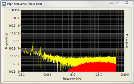
GUID-386AB9AD-3F1D-49A4-807C-E7B2BA656262-low.png
Figure 8-11 PCIe 3.0 Phase Jitter, 100-MHz HCSL
GUID-7B1A7BD7-51D6-4F39-A08E-30503D96235C-low.png
Figure 8-12 PCIe 3.0 RMS Jitter, 100-MHz HCSL