SNAS522K September   2011  – December 2023 LMK03806

PRODUCTION DATA  

  1.   1
  2. Features
  3. Applications
  4. Description
  5. Pin Configuration and Functions
  6. Specifications
    1. 5.1 Absolute Maximum Ratings
    2. 5.2 ESD Ratings
    3. 5.3 Recommended Operating Conditions
    4. 5.4 Thermal Information
    5. 5.5 Electrical Characteristics
    6. 5.6 Timing Requirements
    7. 5.7 Typical Characteristics
  7. Parameter Measurement Information
    1. 6.1 Differential Voltage Measurement Terminology
  8. Detailed Description
    1. 7.1 Overview
    2. 7.2 Functional Block Diagrams
    3. 7.3 Features Description
      1. 7.3.1 Serial MICROWIRE Timing Diagram and Terminology
      2. 7.3.2 Crystal Support With Buffered Outputs
      3. 7.3.3 Integrated Loop Filter Poles
      4. 7.3.4 Integrated VCO
      5. 7.3.5 Clock Distribution
        1. 7.3.5.1 CLKout DIvider
        2. 7.3.5.2 Programmable Output Type
        3. 7.3.5.3 Clock Output Synchronization
      6. 7.3.6 Default Start-Up Clocks
    4. 7.4 Device Functional Modes
    5. 7.5 Programming
      1. 7.5.1 General Information
        1. 7.5.1.1 Special Programming Case for R0 to R5 for CLKoutX_Y_DIV > 25
        2. 7.5.1.2 Recommended Initial Programming Sequence
        3. 7.5.1.3 READBACK
          1. 7.5.1.3.1 Readback Example
  9. Application and Implementation
    1. 8.1 Application Information
      1. 8.1.1 Crystal Interface
      2. 8.1.2 Driving OSCin Pins With a Single-Ended Source
      3. 8.1.3 Driving OSCin Pins With a Differential Source
      4. 8.1.4 Frequency Planning With the LMK03806
      5. 8.1.5 Configuring the PLL
        1. 8.1.5.1 Example PLL Configuration
      6. 8.1.6 Digital Lock Detect
    2. 8.2 Typical Application
      1. 8.2.1 Design Requirements
      2. 8.2.2 Detailed Design Procedure
        1. 8.2.2.1 Device Selection
          1. 8.2.2.1.1 Clock Architect
          2. 8.2.2.1.2 Clock Design Tool
          3. 8.2.2.1.3 Calculation Using LCM
        2. 8.2.2.2 Device Configuration
        3. 8.2.2.3 PLL Loop Filter Design
          1. 8.2.2.3.1 Example Loop Filter Design
        4. 8.2.2.4 Other Device Specific Configuration
          1. 8.2.2.4.1 Digital Lock Detect
        5. 8.2.2.5 Device Programming
      3. 8.2.3 Application Curves
    3. 8.3 System Examples
      1. 8.3.1 System Level Diagram
    4. 8.4 Best Design Practices
      1. 8.4.1 LVCMOS Complementary vs. Non-Complementary Operation
      2. 8.4.2 LVPECL Outputs
      3. 8.4.3 Sharing MICROWIRE (SPI) Lines
      4. 8.4.4 SYNC Pin
      5. 8.4.5 CLKout Vcc Pins
    5. 8.5 Power Supply Recommendations
      1. 8.5.1 Current Consumption and Power Dissipation Calculations
    6. 8.6 Layout
      1. 8.6.1 Layout Guidelines
      2. 8.6.2 Layout Example
  10. Device and Documentation Support
    1. 9.1 Device Support
      1. 9.1.1 Development Support
    2. 9.2 Documentation Support
      1. 9.2.1 Related Documentation
    3. 9.3 Receiving Notification of Documentation Updates
    4. 9.4 Support Resources
    5. 9.5 Trademarks
    6. 9.6 Electrostatic Discharge Caution
    7. 9.7 Glossary
  11. 10Register Maps
    1. 10.1  Default Device Register Settings After Power On Reset
    2. 10.2  Register R0 TO R5
      1. 10.2.1 CLKoutX_Y_PD, Powerdown CLKoutX_Y Output Path
      2. 10.2.2 RESET
      3. 10.2.3 POWERDOWN
      4. 10.2.4 CLKoutX_Y_DIV, Clock Output Divide
    3. 10.3  Registers R6 TO R8
      1. 10.3.1 CLKoutX_TYPE
    4. 10.4  REGISTER R9
    5. 10.5  REGISTER R10
      1. 10.5.1 OSCout1_TYPE, LVPECL Output Amplitude Control
      2. 10.5.2 OSCout0_TYPE
      3. 10.5.3 EN_OSCoutX, OSCout Output Enable
      4. 10.5.4 OSCoutX_MUX, Clock Output Mux
      5. 10.5.5 OSCout_DIV, Oscillator Output Divide
    6. 10.6  REGISTER R11
      1. 10.6.1 NO_SYNC_CLKoutX_Y
      2. 10.6.2 SYNC_POL_INV
      3. 10.6.3 SYNC_TYPE
      4. 10.6.4 EN_PLL_XTAL
    7. 10.7  REGISTER R12
      1. 10.7.1 LD_MUX
      2. 10.7.2 LD_TYPE
      3. 10.7.3 SYNC_PLL_DLD
    8. 10.8  REGISTER R13
      1. 10.8.1 READBACK_TYPE
      2. 10.8.2 GPout0
    9. 10.9  REGISTER 14
      1. 10.9.1 GPout1
    10. 10.10 REGISTER 16
    11. 10.11 REGISTER 24
      1. 10.11.1 PLL_C4_LF, PLL Integrated Loop Filter Component
      2. 10.11.2 PLL_C3_LF, PLL Integrated Loop Filter Component
      3. 10.11.3 PLL_R4_LF, PLL Integrated Loop Filter Component
      4. 10.11.4 PLL_R3_LF, PLL Integrated Loop Filter Component
    12. 10.12 REGISTER 26
      1. 10.12.1 EN_PLL_REF_2X, PLL Reference Frequency Doubler
      2. 10.12.2 PLL_CP_GAIN, PLL Charge Pump Current
      3. 10.12.3 PLL_DLD_CNT
    13. 10.13 REGISTER 28
      1. 10.13.1 PLL_R, PLL R Divider
    14. 10.14 REGISTER 29
      1. 10.14.1 OSCin_FREQ, PLL Oscillator Input Frequency Register
      2. 10.14.2 PLL_N_CAL, PLL N Calibration Divider
    15. 10.15 REGISTER 30
      1. 10.15.1 PLL_P, PLL N Prescaler Divider
      2. 10.15.2 PLL_N, PLL N Divider
    16. 10.16 REGISTER 31
      1. 10.16.1 READBACK_ADDR
      2. 10.16.2 uWire_LOCK
  12. 11Revision History
  13. 12Mechanical, Packaging, and Orderable Information

Package Options

Mechanical Data (Package|Pins)
Thermal pad, mechanical data (Package|Pins)
Orderable Information

Differential Voltage Measurement Terminology

The differential voltage of a differential signal can be described by two different definitions causing confusion when reading data sheets or communicating with other engineers. This section will address the measurement and description of a differential signal so that the reader will be able to understand and discern between the two different definitions when used.

The first definition used to describe a differential signal is the absolute value of the voltage potential between the inverting and noninverting signal. The symbol for this first measurement is typically VID or VOD depending on if an input or output voltage is being described.

The second definition used to describe a differential signal is to measure the potential of the noninverting signal with respect to the inverting signal. The symbol for this second measurement is VSS and is a calculated parameter. Nowhere in the IC does this signal exist with respect to ground, it only exists in reference to its differential pair. VSS can be measured directly by oscilloscopes with floating references, otherwise this value can be calculated as twice the value of VOD as described in the first description.

Figure 6-1 shows the two different definitions side-by-side for inputs and Figure 6-2 shows the two different definitions side-by-side for outputs. The VID and VOD definitions show VA and VB DC levels that the noninverting and inverting signals toggle between with respect to ground. VSS input and output definitions show that if the inverting signal is considered the voltage potential reference, the noninverting signal voltage potential is now increasing and decreasing above and below the noninverting reference. Thus the peak-to-peak voltage of the differential signal can be measured.

VID and VOD are often defined as volts (V) and VSS is often defined as volts peak-to-peak (VPP).
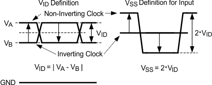
GUID-F00F76C4-9A3E-46F4-B47A-3B3A6E0492B4-low.gifFigure 6-1 Two Different Definitions for Differential Input Signals
GUID-3E8A4178-CB1E-48F3-BB97-1A9D203F570D-low.gifFigure 6-2 Two Different Definitions for Differential Output Signals

Refer to application note AN-912, Common Data Transmission Parameters and their Definitions (SNLA036) for more information.