SNAS522K September 2011 – December 2023 LMK03806
PRODUCTION DATA
- 1
- 1 Features
- 2 Applications
- 3 Description
- 4 Pin Configuration and Functions
- 5 Specifications
- 6 Parameter Measurement Information
-
7 Detailed Description
- 7.1 Overview
- 7.2 Functional Block Diagrams
- 7.3 Features Description
- 7.4 Device Functional Modes
- 7.5 Programming
-
8 Application and Implementation
- 8.1 Application Information
- 8.2 Typical Application
- 8.3 System Examples
- 8.4 Best Design Practices
- 8.5 Power Supply Recommendations
- 8.6 Layout
- 9 Device and Documentation Support
-
10Register Maps
- 10.1 Default Device Register Settings After Power On Reset
- 10.2 Register R0 TO R5
- 10.3 Registers R6 TO R8
- 10.4 REGISTER R9
- 10.5 REGISTER R10
- 10.6 REGISTER R11
- 10.7 REGISTER R12
- 10.8 REGISTER R13
- 10.9 REGISTER 14
- 10.10 REGISTER 16
- 10.11 REGISTER 24
- 10.12 REGISTER 26
- 10.13 REGISTER 28
- 10.14 REGISTER 29
- 10.15 REGISTER 30
- 10.16 REGISTER 31
- 11Revision History
- 12Mechanical, Packaging, and Orderable Information
Package Options
Mechanical Data (Package|Pins)
- NKD|64
Thermal pad, mechanical data (Package|Pins)
- NKD|64
Orderable Information
8.6.1 Layout Guidelines
Power consumption of the LMK03806 can be high enough to require attention to thermal management. For reliability and performance reasons the die temperature should be limited to a maximum of 125°C. That is, as an estimate, TA (ambient temperature) plus device power consumption times θJA should not exceed 125°C.
The package of the device has an exposed pad that provides the primary heat removal path as well as excellent electrical grounding to a printed-circuit-board. To maximize the removal of heat from the package a thermal land pattern including multiple vias to a ground plane must be incorporated on the PCB within the footprint of the package. The exposed pad must be soldered down to ensure adequate heat conduction out of the package.
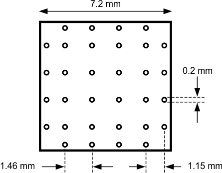
A recommended land and via pattern is shown in Figure 8-14. More information on soldering WQFN packages and gerber footprints can be obtained: http://www.ti.com/packaging.
A recommended footprint including recommended solder mask and solder paste layers can be found at: http://www.ti.com/packaging for the NKD0064A package.
 Figure 8-14 Recommended Land and Via Pattern
To minimize junction temperature, TI recommends that a simple heat sink be built into the PCB (if the ground plane layer is not exposed). This is done by including a copper area of about 2 square inches on the opposite side of the PCB from the device. This copper area may be plated or solder coated to prevent corrosion but should not have conformal coating (if possible), which could provide thermal insulation. The vias shown in Figure 8-14 should connect these top and bottom copper layers and to the ground layer. These vias act as heat pipes to carry the thermal energy away from the device side of the board to where it can be more effectively dissipated.