SNAS840 may   2023 LMK04368-EP

PRODUCTION DATA  

  1. Features
  2. Applications
  3. Description
  4. Revision History
  5. Pin Configuration and Functions
  6. Specifications
    1. 6.1 Absolute Maximum Ratings
    2. 6.2 ESD Ratings
    3. 6.3 Recommended Operating Conditions
    4. 6.4 Thermal Information
    5. 6.5 Electrical Characteristics
    6. 6.6 Timing Requirements
    7. 6.7 Timing Diagram
    8. 6.8 Typical Characteristics
  7. Parameter Measurement Information
    1. 7.1 Charge Pump Current Specification Definitions
      1. 7.1.1 Charge Pump Output Current Magnitude Variation vs Charge Pump Output Voltage
      2. 7.1.2 Charge Pump Sink Current vs Charge Pump Output Source Current Mismatch
      3. 7.1.3 Charge Pump Output Current Magnitude Variation vs Ambient Temperature
    2. 7.2 Differential Voltage Measurement Terminology
  8. Detailed Description
    1. 8.1 Overview
      1. 8.1.1 Differences from the LMK04832
        1. 8.1.1.1 Jitter Cleaning
        2. 8.1.1.2 JEDEC JESD204B/C Support
      2. 8.1.2 Clock Inputs
        1. 8.1.2.1 Inputs for PLL1
        2. 8.1.2.2 Inputs for PLL2
        3. 8.1.2.3 Inputs When Using Clock Distribution Mode
      3. 8.1.3 PLL1
        1. 8.1.3.1 Frequency Holdover
        2. 8.1.3.2 External VCXO for PLL1
      4. 8.1.4 PLL2
        1. 8.1.4.1 Internal VCOs for PLL2
        2. 8.1.4.2 External VCO Mode
      5. 8.1.5 Clock Distribution
        1. 8.1.5.1 Clock Divider
        2. 8.1.5.2 High Performance Divider Bypass Mode
        3. 8.1.5.3 SYSREF Clock Divider
        4. 8.1.5.4 Device Clock Delay
        5. 8.1.5.5 Dynamic Digital Delay
        6. 8.1.5.6 SYSREF Delay: Global and Local
        7. 8.1.5.7 Programmable Output Formats
        8. 8.1.5.8 Clock Output Synchronization
      6. 8.1.6 0-Delay
      7. 8.1.7 Status Pins
    2. 8.2 Functional Block Diagram
    3. 8.3 Feature Description
      1. 8.3.1 Synchronizing PLL R Dividers
        1. 8.3.1.1 PLL1 R Divider Synchronization
        2. 8.3.1.2 PLL2 R Divider Synchronization
      2. 8.3.2 SYNC/SYSREF
      3. 8.3.3 JEDEC JESD204B/C
        1. 8.3.3.1 How to Enable SYSREF
          1. 8.3.3.1.1 Setup of SYSREF Example
          2. 8.3.3.1.2 SYSREF_CLR
        2. 8.3.3.2 SYSREF Modes
          1. 8.3.3.2.1 SYSREF Pulser
          2. 8.3.3.2.2 Continuous SYSREF
          3. 8.3.3.2.3 SYSREF Request
      4. 8.3.4 Digital Delay
        1. 8.3.4.1 Fixed Digital Delay
        2. 8.3.4.2 Fixed Digital Delay Example
        3. 8.3.4.3 Dynamic Digital Delay
        4. 8.3.4.4 Single and Multiple Dynamic Digital Delay Example
      5. 8.3.5 SYSREF to Device Clock Alignment
      6. 8.3.6 Input Clock Switching
        1. 8.3.6.1 Input Clock Switching - Manual Mode
        2. 8.3.6.2 Input Clock Switching - Pin Select Mode
        3. 8.3.6.3 Input Clock Switching - Automatic Mode
      7. 8.3.7 Digital Lock Detect (DLD)
        1. 8.3.7.1 Calculating Digital Lock Detect Frequency Accuracy
      8. 8.3.8 Holdover
        1. 8.3.8.1 Enable Holdover
          1. 8.3.8.1.1 Fixed (Manual) CPout1 Holdover Mode
          2. 8.3.8.1.2 Tracked CPout1 Holdover Mode
        2. 8.3.8.2 During Holdover
        3. 8.3.8.3 Exiting Holdover
        4. 8.3.8.4 Holdover Frequency Accuracy and DAC Performance
      9. 8.3.9 PLL2 Loop Filter
    4. 8.4 Device Functional Modes
      1. 8.4.1 DUAL PLL
        1. 8.4.1.1 Dual Loop
        2. 8.4.1.2 Dual Loop With Cascaded 0-Delay
        3. 8.4.1.3 Dual Loop With Nested 0-Delay
      2. 8.4.2 Single PLL
        1. 8.4.2.1 PLL2 Single Loop
          1. 8.4.2.1.1 PLL2 Single Loop With 0-Delay
        2. 8.4.2.2 PLL2 With an External VCO
      3. 8.4.3 Distribution Mode
    5. 8.5 Programming
      1. 8.5.1 Recommended Programming Sequence
    6. 8.6 Register Maps
      1. 8.6.1 Register Map for Device Programming
      2. 8.6.2 Device Register Descriptions
        1. 8.6.2.1 System Functions
          1. 8.6.2.1.1 RESET, SPI_3WIRE_DIS
          2. 8.6.2.1.2 POWERDOWN
          3. 8.6.2.1.3 ID_DEVICE_TYPE
          4. 8.6.2.1.4 ID_PROD
          5. 8.6.2.1.5 ID_MASKREV
          6. 8.6.2.1.6 ID_VNDR
        2. 8.6.2.2 (0x100 to 0x137) Device Clock and SYSREF Clock Output Controls
          1. 8.6.2.2.1 DCLKX_Y_DIV
          2. 8.6.2.2.2 DCLKX_Y_DDLY
          3. 8.6.2.2.3 CLKoutX_Y_PD, CLKoutX_Y_ODL, CLKoutX_Y_IDL, DCLKX_Y_DDLY_PD, DCLKX_Y_DDLY[9:8], DCLKX_Y_DIV[9:8]
          4. 8.6.2.2.4 CLKoutX_SRC_MUX, DCLKX_Y_PD, DCLKX_Y_BYP, DCLKX_Y_DCC, DCLKX_Y_POL, DCLKX_Y_HS
          5. 8.6.2.2.5 CLKoutY_SRC_MUX, SCLKX_Y_PD, SCLKX_Y_DIS_MODE, SCLKX_Y_POL, SCLKX_Y_HS
          6. 8.6.2.2.6 SCLKX_Y_ADLY_EN, SCLKX_Y_ADLY
          7. 8.6.2.2.7 SCLKX_Y_DDLY
          8. 8.6.2.2.8 CLKoutY_FMT, CLKoutX_FMT
        3. 8.6.2.3 SYSREF, SYNC, and Device Config
          1. 8.6.2.3.1  VCO_MUX, OSCout_MUX, OSCout_FMT
          2. 8.6.2.3.2  SYSREF_REQ_EN, SYNC_BYPASS, SYSREF_MUX
          3. 8.6.2.3.3  SYSREF_DIV
          4. 8.6.2.3.4  SYSREF_DDLY
          5. 8.6.2.3.5  SYSREF_PULSE_CNT
          6. 8.6.2.3.6  PLL2_RCLK_MUX, PLL2_NCLK_MUX, PLL1_NCLK_MUX, FB_MUX, FB_MUX_EN
          7. 8.6.2.3.7  PLL1_PD, VCO_LDO_PD, VCO_PD, OSCin_PD, SYSREF_GBL_PD, SYSREF_PD, SYSREF_DDLY_PD, SYSREF_PLSR_PD
          8. 8.6.2.3.8  DDLYdSYSREF_EN, DDLYdX_EN
          9. 8.6.2.3.9  DDLYd_STEP_CNT
          10. 8.6.2.3.10 SYSREF_CLR, SYNC_1SHOT_EN, SYNC_POL, SYNC_EN, SYNC_PLL2_DLD, SYNC_PLL1_DLD, SYNC_MODE
          11. 8.6.2.3.11 SYNC_DISSYSREF, SYNC_DISX
          12. 8.6.2.3.12 PLL1R_SYNC_EN, PLL1R_SYNC_SRC, PLL2R_SYNC_EN, FIN0_DIV2_EN, FIN0_INPUT_TYPE
        4. 8.6.2.4 (0x146 - 0x149) CLKIN Control
          1. 8.6.2.4.1 CLKin_SEL_PIN_EN, CLKin_SEL_PIN_POL, CLKin2_EN, CLKin1_EN, CLKin0_EN, CLKin2_TYPE, CLKin1_TYPE, CLKin0_TYPE
          2. 8.6.2.4.2 CLKin_SEL_AUTO_REVERT_EN, CLKin_SEL_AUTO_EN, CLKin_SEL_MANUAL, CLKin1_DEMUX, CLKin0_DEMUX
          3. 8.6.2.4.3 CLKin_SEL0_MUX, CLKin_SEL0_TYPE
          4. 8.6.2.4.4 SDIO_RDBK_TYPE, CLKin_SEL1_MUX, CLKin_SEL1_TYPE
        5. 8.6.2.5 RESET_MUX, RESET_TYPE
        6. 8.6.2.6 (0x14B - 0x152) Holdover
          1. 8.6.2.6.1 LOS_TIMEOUT, LOS_EN, TRACK_EN, HOLDOVER_FORCE, MAN_DAC_EN, MAN_DAC[9:8]
          2. 8.6.2.6.2 MAN_DAC
          3. 8.6.2.6.3 DAC_TRIP_LOW
          4. 8.6.2.6.4 DAC_CLK_MULT, DAC_TRIP_HIGH
          5. 8.6.2.6.5 DAC_CLK_CNTR
          6. 8.6.2.6.6 CLKin_OVERRIDE, HOLDOVER_EXIT_MODE, HOLDOVER_PLL1_DET, LOS_EXTERNAL_INPUT, HOLDOVER_VTUNE_DET, CLKin_SWITCH_CP_TRI, HOLDOVER_EN
          7. 8.6.2.6.7 HOLDOVER_DLD_CNT
        7. 8.6.2.7 (0x153 - 0x15F) PLL1 Configuration
          1. 8.6.2.7.1 CLKin0_R
          2. 8.6.2.7.2 CLKin1_R
          3. 8.6.2.7.3 CLKin2_R
          4. 8.6.2.7.4 PLL1_N
          5. 8.6.2.7.5 PLL1_WND_SIZE, PLL1_CP_TRI, PLL1_CP_POL, PLL1_CP_GAIN
          6. 8.6.2.7.6 PLL1_DLD_CNT
          7. 8.6.2.7.7 HOLDOVER_EXIT_NADJ
          8. 8.6.2.7.8 PLL1_LD_MUX, PLL1_LD_TYPE
        8. 8.6.2.8 (0x160 - 0x16E) PLL2 Configuration
          1. 8.6.2.8.1 PLL2_R
          2. 8.6.2.8.2 PLL2_P, OSCin_FREQ, PLL2_REF_2X_EN
          3. 8.6.2.8.3 PLL2_N_CAL
          4. 8.6.2.8.4 PLL2_N
          5. 8.6.2.8.5 PLL2_WND_SIZE, PLL2_CP_GAIN, PLL2_CP_POL, PLL2_CP_TRI
          6. 8.6.2.8.6 PLL2_DLD_CNT
          7. 8.6.2.8.7 PLL2_LD_MUX, PLL2_LD_TYPE
        9. 8.6.2.9 (0x16F - 0x555) Misc Registers
          1. 8.6.2.9.1 PLL2_PRE_PD, PLL2_PD, FIN0_PD
          2. 8.6.2.9.2 PLL1R_RST
          3. 8.6.2.9.3 CLR_PLL1_LD_LOST, CLR_PLL2_LD_LOST
          4. 8.6.2.9.4 RB_PLL1_LD_LOST, RB_PLL1_LD, RB_PLL2_LD_LOST, RB_PLL2_LD
          5. 8.6.2.9.5 RB_DAC_VALUE (MSB), RB_CLKinX_SEL, RB_CLKinX_LOS
          6. 8.6.2.9.6 RB_DAC_VALUE
          7. 8.6.2.9.7 RB_HOLDOVER
          8. 8.6.2.9.8 SPI_LOCK
  9. Application and Implementation
    1. 9.1 Application Information
      1. 9.1.1 Treatment of Unused Pins
      2. 9.1.2 Digital Lock Detect Frequency Accuracy
        1. 9.1.2.1 Minimum Lock Time Calculation Example
      3. 9.1.3 Driving CLKIN AND OSCIN Inputs
        1. 9.1.3.1 Driving CLKIN and OSCIN PINS With a Differential Source
        2. 9.1.3.2 Driving CLKIN Pins With a Single-Ended Source
      4. 9.1.4 Termination and Use of Clock Output Drivers
        1. 9.1.4.1 Termination for DC Coupled Differential Operation
        2. 9.1.4.2 Termination for AC Coupled Differential Operation
        3. 9.1.4.3 Termination for Single-Ended Operation
      5. 9.1.5 Output Termination and Biasing
        1. 9.1.5.1 LVPECL
        2. 9.1.5.2 LVDS/HSDS
        3. 9.1.5.3 CML
      6. 9.1.6 OSCin Doubler for Best Phase Noise Performance
    2. 9.2 Typical Application
      1. 9.2.1 Design Requirements
      2. 9.2.2 Detailed Design Procedure
        1. 9.2.2.1 Device Selection
        2. 9.2.2.2 Device Configuration and Simulation
        3. 9.2.2.3 Device Setup
      3. 9.2.3 Application Curve
    3. 9.3 System Examples
      1. 9.3.1 System Level Diagram
    4. 9.4 Power Supply Recommendations
      1. 9.4.1 Current Consumption
    5. 9.5 Layout
      1. 9.5.1 Thermal Management
      2. 9.5.2 Layout Guidelines
      3. 9.5.3 Layout Example
  10. 10Device and Documentation Support
    1. 10.1 Device Support
      1. 10.1.1 Development Support
        1. 10.1.1.1 Clock Tree Architect
        2. 10.1.1.2 PLLatinum Simulation
        3. 10.1.1.3 TICS Pro
    2. 10.2 Documentation Support
      1. 10.2.1 Related Documentation
    3. 10.3 Receiving Notification of Documentation Updates
    4. 10.4 Support Resources
    5. 10.5 Trademarks
    6. 10.6 Electrostatic Discharge Caution
    7. 10.7 Glossary
  11. 11Mechanical, Packaging, and Orderable Information

Package Options

Mechanical Data (Package|Pins)
Thermal pad, mechanical data (Package|Pins)
Orderable Information

Holdover Frequency Accuracy and DAC Performance

When in holdover mode, PLL1 runs in open loop and the DAC sets the CPout1 voltage. If fixed CPout1 mode is used, then the output of the DAC is dependent upon the MAN_DAC register. If tracked CPout1 mode is used, then the output of the DAC is approximately the same voltage at the CPout1 pin before holdover mode was entered. When using Tracked mode and MAN_DAC_EN = 1, the DAC value during holdover is loaded with the programmed value in MAN_DAC and not the tracked value.

When in Tracked CPout1 mode, the DAC has a worst-case tracking error of ±2 LSBs once PLL1 tuning voltage is acquired. The step size is approximately 3.2 mV, therefore the VCXO frequency error during holdover mode caused by the DAC tracking accuracy is ±6.4 mV × Kv, where Kv is the tuning sensitivity of the VCXO in use. Therefore, the accuracy of the system when in holdover mode in ppm is:

Equation 2. GUID-5E32B7CE-8291-4D1D-9615-675A33BE9FD5-low.gif

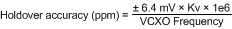
As an example, consider a system with a 19.2-MHz clock input, a 153.6-MHz VCXO with a Kv of 17 kHz/V. The accuracy of the system in holdover in ppm is:

Equation 3. ±0.71 ppm = ±6.4 mV × 17 kHz/V × 1e6 / 153.6 MHz

It is important to account for this frequency error when determining the allowable frequency error window to cause holdover mode to exit.