SNAS859 March 2024 LMK05318B-Q1
PRODUCTION DATA
- 1
- 1 Features
- 2 Applications
- 3 Description
- 4 Pin Configuration and Functions
- 5 Specifications
- 6 Parameter Measurement Information
-
7 Detailed Description
- 7.1 Overview
- 7.2 Functional Block Diagram
- 7.3
Feature Description
- 7.3.1 Oscillator Input (XO_P/N)
- 7.3.2 Reference Inputs (PRIREF_P/N and SECREF_P/N)
- 7.3.3 Clock Input Interfacing and Termination
- 7.3.4 Reference Input Mux Selection
- 7.3.5 Hitless Switching
- 7.3.6 Gapped Clock Support on Reference Inputs
- 7.3.7 Input Clock and PLL Monitoring, Status, and Interrupts
- 7.3.8
PLL Relationships
- 7.3.8.1 PLL Frequency Relationships
- 7.3.8.2 Analog PLLs (APLL1, APLL2)
- 7.3.8.3 APLL Reference Paths
- 7.3.8.4 APLL Phase Frequency Detector (PFD) and Charge Pump
- 7.3.8.5 APLL Feedback Divider Paths
- 7.3.8.6 APLL Loop Filters (LF1, LF2)
- 7.3.8.7 APLL Voltage Controlled Oscillators (VCO1, VCO2)
- 7.3.8.8 APLL VCO Clock Distribution Paths (P1, P2)
- 7.3.8.9 DPLL Reference (R) Divider Paths
- 7.3.8.10 DPLL Time-to-Digital Converter (TDC)
- 7.3.8.11 DPLL Loop Filter (DLF)
- 7.3.8.12 DPLL Feedback (FB) Divider Path
- 7.3.9 Output Clock Distribution
- 7.3.10 Output Channel Muxes
- 7.3.11 Output Dividers (OD)
- 7.3.12 Clock Outputs (OUTx_P/N)
- 7.3.13 Glitchless Output Clock Start-Up
- 7.3.14 Clock Output Interfacing and Termination
- 7.3.15 Output Synchronization (SYNC)
- 7.4 Device Functional Modes
- 7.5 Programming
- 8 Application and Implementation
- 9 Device and Documentation Support
- 10Revision History
- 11Mechanical, Packaging, and Orderable Information
Package Options
Refer to the PDF data sheet for device specific package drawings
Mechanical Data (Package|Pins)
- RGZ|48
Thermal pad, mechanical data (Package|Pins)
- RGZ|48
Orderable Information
8.4.1 Power Supply Bypassing
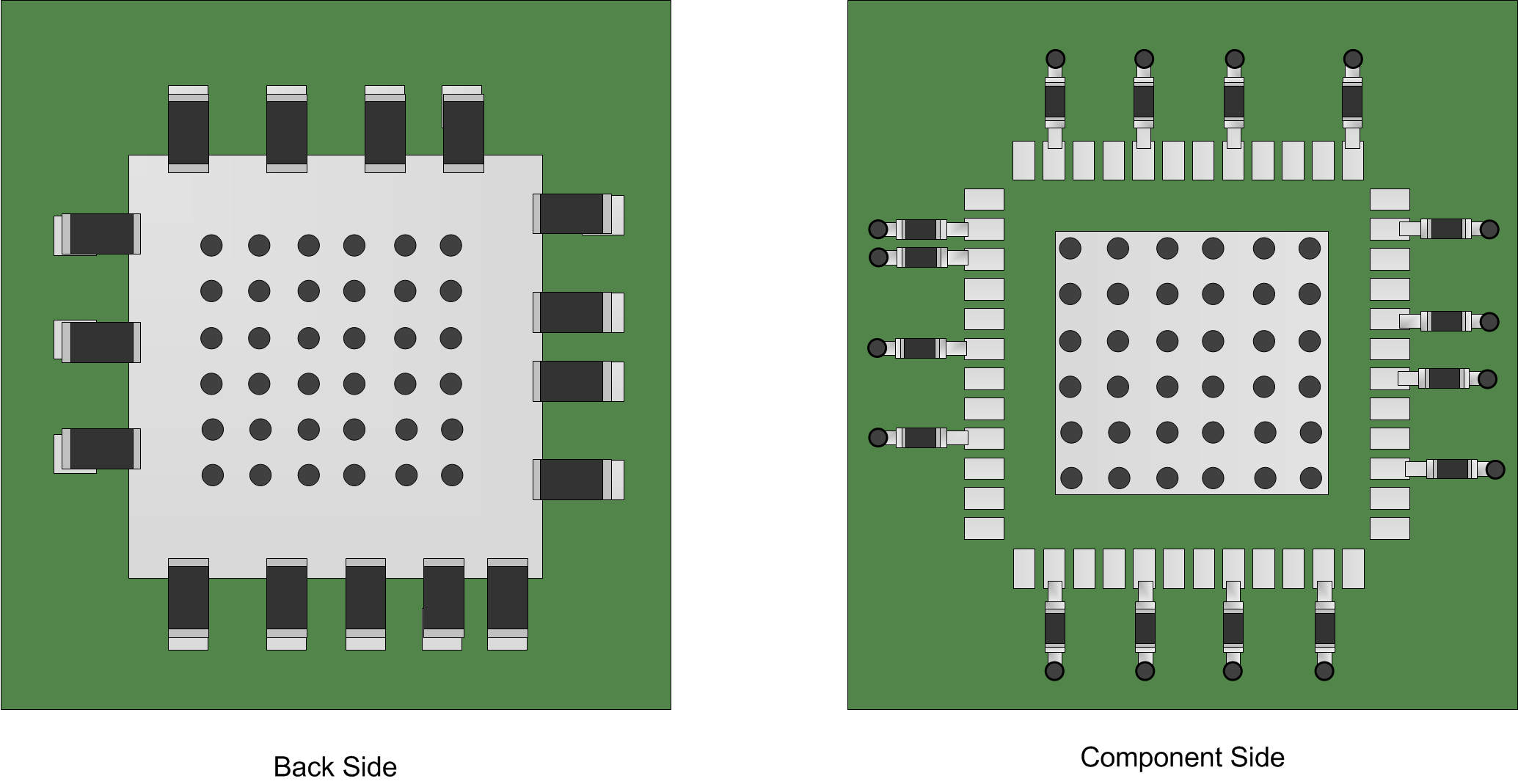
Figure 8-7 shows two general placements of power supply bypass capacitors on either the back side or the component side of the PCB. If the capacitors are mounted on the back side, 0402 components can be employed. For component side mounting, use 0201 body size capacitors to facilitate signal routing. A combination of component side and back side placement can be used. Keep the connections between the bypass capacitors and the power supply on the device as short as possible. Ground the other side of the capacitor using a low-impedance connection to the ground plane.

| (Does not indicate actual location of the LMK05318B-Q1 supply pins) |