SNAS801B June   2020  – June 2021 LMK05318B

PRODUCTION DATA  

  1. Features
  2. Applications
  3. Description
  4. Revision History
  5. Description (continued)
  6. Pin Configuration and Functions
    1. 6.1 Device Start-Up Modes
  7. Specifications
    1. 7.1 Absolute Maximum Ratings
    2. 7.2 ESD Ratings
    3. 7.3 Recommended Operating Conditions
    4. 7.4 Thermal Information: 4-Layer JEDEC Standard PCB
    5. 7.5 Thermal Information: 10-Layer Custom PCB
    6. 7.6 Electrical Characteristics
    7. 7.7 Timing Diagrams
    8. 7.8 Typical Characteristics
  8. Parameter Measurement Information
    1. 8.1 Output Clock Test Configurations
  9. Detailed Description
    1. 9.1 Overview
      1. 9.1.1 ITU-T G.8262 (SyncE) Standards Compliance
    2. 9.2 Functional Block Diagram
      1. 9.2.1 PLL Architecture Overview
      2. 9.2.2 DPLL Mode
      3. 9.2.3 APLL-Only Mode
    3. 9.3 Feature Description
      1. 9.3.1  Oscillator Input (XO_P/N)
      2. 9.3.2  Reference Inputs (PRIREF_P/N and SECREF_P/N)
        1. 9.3.2.1 Programmable Input Hysteresis
      3. 9.3.3  Clock Input Interfacing and Termination
      4. 9.3.4  Reference Input Mux Selection
        1. 9.3.4.1 Automatic Input Selection
        2. 9.3.4.2 Manual Input Selection
      5. 9.3.5  Hitless Switching
        1. 9.3.5.1 Hitless Switching With 1-PPS Inputs
      6. 9.3.6  Gapped Clock Support on Reference Inputs
      7. 9.3.7  Input Clock and PLL Monitoring, Status, and Interrupts
        1. 9.3.7.1 XO Input Monitoring
        2. 9.3.7.2 Reference Input Monitoring
          1. 9.3.7.2.1 Reference Validation Timer
          2. 9.3.7.2.2 Amplitude Monitor
          3. 9.3.7.2.3 Frequency Monitoring
          4. 9.3.7.2.4 Missing Pulse Monitor (Late Detect)
          5. 9.3.7.2.5 Runt Pulse Monitor (Early Detect)
          6. 9.3.7.2.6 Phase Valid Monitor for 1-PPS Inputs
        3. 9.3.7.3 PLL Lock Detectors
        4. 9.3.7.4 Tuning Word History
        5. 9.3.7.5 Status Outputs
        6. 9.3.7.6 Interrupt
      8. 9.3.8  PLL Relationships
        1. 9.3.8.1  PLL Frequency Relationships
        2. 9.3.8.2  Analog PLLs (APLL1, APLL2)
        3. 9.3.8.3  APLL Reference Paths
          1. 9.3.8.3.1 APLL XO Doubler
          2. 9.3.8.3.2 APLL1 XO Reference (R) Divider
          3. 9.3.8.3.3 APLL2 Reference (R) Dividers
        4. 9.3.8.4  APLL Phase Frequency Detector (PFD) and Charge Pump
        5. 9.3.8.5  APLL Feedback Divider Paths
          1. 9.3.8.5.1 APLL1 N Divider With SDM
          2. 9.3.8.5.2 APLL2 N Divider With SDM
        6. 9.3.8.6  APLL Loop Filters (LF1, LF2)
        7. 9.3.8.7  APLL Voltage Controlled Oscillators (VCO1, VCO2)
          1. 9.3.8.7.1 VCO Calibration
        8. 9.3.8.8  APLL VCO Clock Distribution Paths (P1, P2)
        9. 9.3.8.9  DPLL Reference (R) Divider Paths
        10. 9.3.8.10 DPLL Time-to-Digital Converter (TDC)
        11. 9.3.8.11 DPLL Loop Filter (DLF)
        12. 9.3.8.12 DPLL Feedback (FB) Divider Path
      9. 9.3.9  Output Clock Distribution
      10. 9.3.10 Output Channel Muxes
      11. 9.3.11 Output Dividers (OD)
      12. 9.3.12 Clock Outputs (OUTx_P/N)
        1. 9.3.12.1 AC-Differential Output (AC-DIFF)
        2. 9.3.12.2 HCSL Output
        3. 9.3.12.3 1.8-V LVCMOS Output
        4. 9.3.12.4 Output Auto-Mute During LOL
      13. 9.3.13 Glitchless Output Clock Start-Up
      14. 9.3.14 Clock Output Interfacing and Termination
      15. 9.3.15 Output Synchronization (SYNC)
      16. 9.3.16 Zero-Delay Mode (ZDM) Synchronization for 1-PPS Input and Output
    4. 9.4 Device Functional Modes
      1. 9.4.1 Device Start-Up Modes
        1. 9.4.1.1 EEPROM Mode
        2. 9.4.1.2 ROM Mode
      2. 9.4.2 PLL Operating Modes
        1. 9.4.2.1 Free-Run Mode
        2. 9.4.2.2 Lock Acquisition
        3. 9.4.2.3 Locked Mode
        4. 9.4.2.4 Holdover Mode
      3. 9.4.3 PLL Start-Up Sequence
      4. 9.4.4 Digitally-Controlled Oscillator (DCO) Mode
        1. 9.4.4.1 DCO Frequency Step Size
        2. 9.4.4.2 DCO Direct-Write Mode
      5. 9.4.5 Zero-Delay Mode Synchronization
    5. 9.5 Programming
      1. 9.5.1 Interface and Control
      2. 9.5.2 I2C Serial Interface
        1. 9.5.2.1 I2C Block Register Transfers
      3. 9.5.3 SPI Serial Interface
        1. 9.5.3.1 SPI Block Register Transfer
      4. 9.5.4 Register Map and EEPROM Map Generation
      5. 9.5.5 General Register Programming Sequence
      6. 9.5.6 EEPROM Programming Flow
        1. 9.5.6.1 EEPROM Programming Using Method #1 (Register Commit)
          1. 9.5.6.1.1 Write SRAM Using Register Commit
          2. 9.5.6.1.2 Program EEPROM
        2. 9.5.6.2 EEPROM Programming Using Method #2 (Direct Writes)
          1. 9.5.6.2.1 Write SRAM Using Direct Writes
          2. 9.5.6.2.2 User-Programmable Fields In EEPROM
      7. 9.5.7 Read SRAM
      8. 9.5.8 Read EEPROM
      9. 9.5.9 EEPROM Start-Up Mode Default Configuration
  10. 10Application and Implementation
    1. 10.1 Application Information
      1. 10.1.1 Device Start-Up Sequence
      2. 10.1.2 Power Down (PDN) Pin
      3. 10.1.3 Power Rail Sequencing, Power Supply Ramp Rate, and Mixing Supply Domains
        1. 10.1.3.1 Mixing Supplies
        2. 10.1.3.2 Power-On Reset (POR) Circuit
        3. 10.1.3.3 Powering Up From a Single-Supply Rail
        4. 10.1.3.4 Power Up From Split-Supply Rails
        5. 10.1.3.5 Non-Monotonic or Slow Power-Up Supply Ramp
      4. 10.1.4 Slow or Delayed XO Start-Up
    2. 10.2 Typical Application
      1. 10.2.1 Design Requirements
      2. 10.2.2 Detailed Design Procedure
      3. 10.2.3 Application Curves
    3. 10.3 Do's and Don'ts
  11. 11Power Supply Recommendations
    1. 11.1 Power Supply Bypassing
    2. 11.2 Device Current and Power Consumption
      1. 11.2.1 Current Consumption Calculations
      2. 11.2.2 Power Consumption Calculations
      3. 11.2.3 Example
  12. 12Layout
    1. 12.1 Layout Guidelines
    2. 12.2 Layout Example
    3. 12.3 Thermal Reliability
      1. 12.3.1 Support for PCB Temperature up to 105 °C
  13. 13Device and Documentation Support
    1. 13.1 Device Support
      1. 13.1.1 TICS Pro
      2. 13.1.2 Related Documentation
    2. 13.2 Receiving Notification of Documentation Updates
    3. 13.3 Support Resources
    4. 13.4 Trademarks
    5. 13.5 Electrostatic Discharge Caution
    6. 13.6 Glossary
  14. 14Mechanical, Packaging, and Orderable Information

Package Options

Mechanical Data (Package|Pins)
Thermal pad, mechanical data (Package|Pins)
Orderable Information

Zero-Delay Mode (ZDM) Synchronization for 1-PPS Input and Output

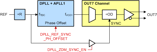
Zero-delay mode synchronization can be enabled to achieve deterministic (+/-1 VCO cycle) input-output phase delay between the selected DPLL reference input clock and the OUT7 clock as shown in Figure 9-31. This is primarily used to achieve deterministic phase relationship between a 1-PPS input and 1-PPS output. This feature can be configured through registers by enabling ZDM (DPLL_ZDM_SYNC_EN bit = 1) and enabling OUT7 divider synchronization (CH7_SYNC_EN bit = 1). The OUT7 clock must be derived from the DPLL and APLL1 VCO domain (fVCO1).

When the DPLL is not locked and the DPLL reference input is invalid, the OUT7 clock is held in mute state (no clock). Once the reference input is validated and selected, the OUT7 channel divider is reset or SYNCed using the DPLL reference input clock edge to achieve a deterministic phase relationship between the reference input and OUT7 clock. OUT7 is not affected by normal output SYNC events, and OUT[0:6] are not be affected by a ZDM SYNC event. The input-to-output phase offset can be adjusted through the DPLL phase offset register control (DPLL_REF_SYNC_PH_OFFSET bits). If the DPLL phase offset is programmed on-the-fly with 1-PPS input, it can take a long time to adjust due to the narrow DPLL bandwidth (10 mHz typical).

Hitless switching between 1-PPS inputs is not supported when ZDM is enabled. If a switchover event between 1-PPS inputs occurs when ZDM is enabled, a soft-reset should be issued for the DPLL to relock and realign the 1-PPS output to the selected input.
GUID-8DADF540-3F7A-47E7-9F40-1AACB0485FF4-low.gifFigure 9-31 DPLL ZDM Synchronization Between Reference Input and OUT7