SNAS822B September 2021 – June 2023 LMK1D2102 , LMK1D2104
PRODUCTION DATA
- 1
- 1 Features
- 2 Applications
- 3 Description
- 4 Revision History
- 5 Device Comparison
- 6 Pin Configuration and Functions
- 7 Specifications
- 8 Parameter Measurement Information
- 9 Detailed Description
- 10Application and Implementation
- 11Device and Documentation Support
- 12Mechanical, Packaging, and Orderable Information
Package Options
Mechanical Data (Package|Pins)
- RGT|16
Thermal pad, mechanical data (Package|Pins)
- RGT|16
Orderable Information
10.2.3 Application Curves
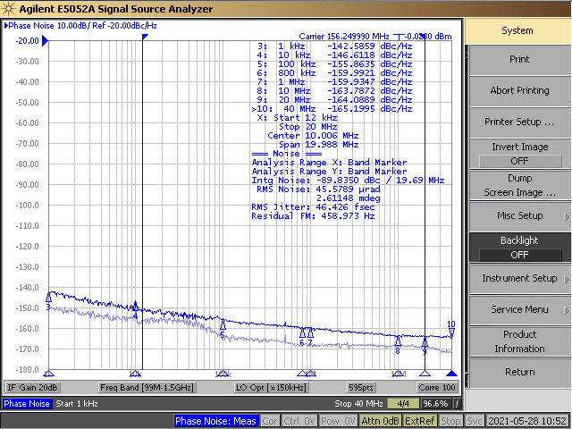
The LMK1D2104's low additive noise is shown below. The low noise 156.25-MHz source with 24-fs RMS jitter shown in Figure 10-3 drives the LMK1D2104, resulting in 46.4-fs RMS when integrated from 12 kHz to 20 MHz (Figure 10-4). The resultant additive jitter is a low 39.7-fs RMS for this configuration. Note that this result applies to the LMK1D2102 device as well.

| Reference signal is low-noise Rohde and Schwarz SMA100B |
 Figure 10-4 LMK1D2104
Output Phase Noise, 156.25 MHz, 46.4-fs RMS (12 kHz to 20 MHz)
Figure 10-4 LMK1D2104
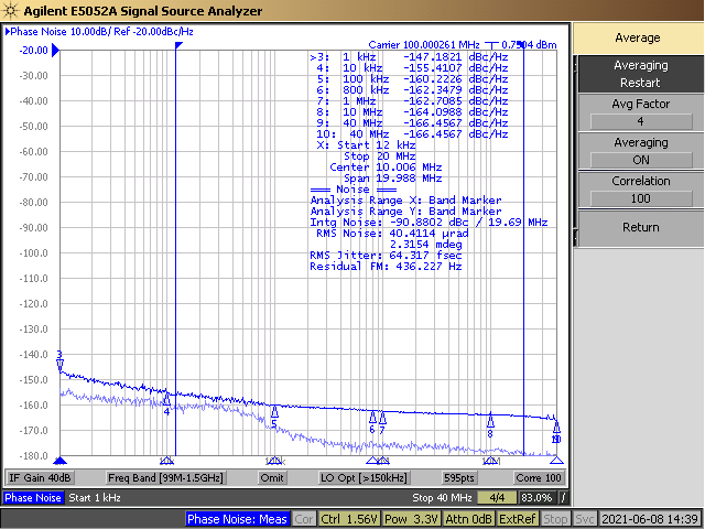
Output Phase Noise, 156.25 MHz, 46.4-fs RMS (12 kHz to 20 MHz)The Figure 10-5 captures the low close-in phase noise of the LMK1D2104 device. The LMK1D2102 and LMK1D2104 have excellent flicker noise as a result of superior process technology and design. This enables their use for clock distribution in radar systems, medical imaging systems etc which require ultra-low close-in phase noise clocks.
 Figure 10-5 LMK1D2104
Output Phase Noise, 100 MHz, 1 kHz offset: -147 dBc/Hz