SNAS880 December 2024 LMK3C0105
PRODUCTION DATA
- 1
- 1 Features
- 2 Applications
- 3 Description
- 4 Pin Configuration and Functions
- 5 Specifications
- 6 Parameter Measurement Information
- 7 Detailed Description
-
8 Device Registers
- 8.1
Register Maps
- 8.1.1 R0 Register (Address = 0x0) [reset = 0x0861/0x0863]
- 8.1.2 R1 Register (Address = 0x1) [reset = 0x5599]
- 8.1.3 R2 Register (Address = 0x2) [reset = 0xC28F]
- 8.1.4 R3 Register (Address = 0x3) [reset = 0x1804]
- 8.1.5 R4 Register (Address = 0x4) [reset = 0x0000]
- 8.1.6 R5 Register (Address = 0x5) [reset = 0x0000]
- 8.1.7 R6 Register (Address = 0x6) [reset = 0x0AA7]
- 8.1.8 R7 Register (Address = 0x7) [reset = 0x5D1F]
- 8.1.9 R8 Register (Address = 0x8) [reset = 0xC28F]
- 8.1.10 R9 Register (Address = 0x9) [reset = 0x3000/0x1000]
- 8.1.11 R10 Register (Address = 0xA) [reset = 0x0010]
- 8.1.12 R11 Register (Address = 0xB) [reset = 0x0000]
- 8.1.13 R12 Register (Address = 0xC) [reset = 0xE800]
- 8.1.14 R238 Register (Address = 0xEE) [reset = 0x0000]
- 8.1
Register Maps
- 9 Application and Implementation
- 10Device and Documentation Support
- 11Revision History
- 12Mechanical, Packaging, and Orderable Information
Refer to the PDF data sheet for device specific package drawings
Mechanical Data (Package|Pins)
- RER|16
Thermal pad, mechanical data (Package|Pins)
7.5.1 I2C Serial Interface
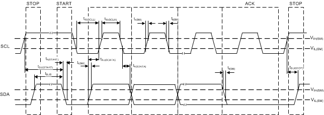
The I2C port on the LMK3C0105 works as a peripheral device and supports both the 100kHz standard mode and 400kHz fast-mode operations. Fast mode imposes a glitch tolerance requirement on the control signals. Therefore, the input receivers ignore pulses of less than 50ns duration. The I2C timing requirements are provided in the I2C Interface Specification. Figure 7-5 shows the timing diagram.
 Figure 7-5 I2C Timing Diagram
The LMK3C0105 is accessed through a 7-bit peripheral address transmitted as part of an I2C packet. Only the device with a matching peripheral address responds to subsequent I2C commands. In I2C mode, the LMK3C0105 allows up to four unique peripheral devices to occupy the I2C bus based on the pin strapping of I2C_ADDR (tied to VDD, GND, SDA, or SCL). By default, the device peripheral address is 0b11010xx (the two LSBs are determined by the I2C_ADDR pin). The full address can be configured through I2C.
During the data transfer through the I2C interface, one clock pulse is generated for each data bit transferred. The data on the SDA line must be stable during the high period of the clock. The high or low state of the data line can change only when the clock signal on the SCL line is low. The start data transfer condition is characterized by a high-to-low transition on the SDA line while SCL is high. The stop data transfer condition is characterized by a low-to-high transition on the SDA line while SCL is high. The start and stop conditions are always initiated by the controller. Every byte on the SDA line must be eight bits long. Each byte must be followed by an acknowledge bit and bytes are sent MSB first. The LMK3C0105 has an 8-bit register address, followed by a 16-bit data word.
The acknowledge bit (A) or non-acknowledge bit (A’) is the 9th bit attached to any 8-bit data byte and is always generated by the receiver to inform the transmitter that the byte has been received (when A = 0) or not (when A’ = 0). A = 0 is done by pulling the SDA line low during the 9th clock pulse and A’ = 0 is done by leaving the SDA line high during the 9th clock pulse.
The I2C controller initiates the data transfer by asserting a start condition which initiates a response from all peripheral devices connected to the serial bus. Based on the 8-bit address byte sent by the controller over the SDA line (consisting of the 7-bit peripheral address (MSB first) and an R/W’ bit), the device whose address corresponds to the transmitted address responds by sending an acknowledge bit. All other devices on the bus remain idle while the selected device waits for data transfer with the controller.
After the data transfer occurs, stop conditions are established. In write mode, the controller asserts a stop condition to end data transfer during the 10th clock pulse following the acknowledge bit for the last data byte from the peripheral. In read mode, the controller receives the last data byte from the peripheral but does not pull SDA low during the 9th clock pulse. This is known as a non-acknowledge bit. By receiving the non-acknowledge bit, the peripheral knows the data transfer is finished and enters the idle mode. The controller then takes the data line low during the low period before the 10th clock pulse, and high during the 10th clock pulse to assert a stop condition. Figure 7-6 and Figure 7-7 show the sequence for block writes and block reads using the LMK3C0105, respectively.
 Figure 7-6 Generic Block Write Sequence
 Figure 7-7 Generic Block Read Sequence