SNAS751
December 2023
LMK5C33414A
PRODUCTION DATA
1
1
Features
2
Applications
3
Description
4
Pin Configuration and Functions
5
Specifications
5.1
Absolute Maximum Ratings
5.2
ESD Ratings
5.3
Recommended Operating Conditions
5.4
Thermal Information
5.5
Electrical Characteristics
5.6
Timing Diagrams
5.7
Typical Characteristics
6
Parameter Measurement Information
6.1
Differential Voltage Measurement Terminology
6.2
Output Clock Test Configurations
7
Detailed Description
7.1
Overview
7.2
Functional Block Diagram
7.2.1
PLL Architecture Overview
7.2.2
DPLL
7.2.2.1
Independent DPLL Operation
7.2.2.2
Cascaded DPLL Operation
7.2.2.3
APLL Cascaded with DPLL
7.2.3
APLL-Only Mode
7.3
Feature Description
7.3.1
Oscillator Input (XO)
7.3.2
Reference Inputs
7.3.3
Clock Input Interfacing and Termination
7.3.4
Reference Input Mux Selection
7.3.4.1
Automatic Input Selection
7.3.4.2
Manual Input Selection
7.3.5
Hitless Switching
7.3.5.1
Hitless Switching With Phase Cancellation
7.3.5.2
Hitless Switching With Phase Slew Control
7.3.5.3
Hitless Switching With 1-PPS Inputs
7.3.6
Gapped Clock Support on Reference Inputs
7.3.7
Input Clock and PLL Monitoring, Status, and Interrupts
7.3.7.1
XO Input Monitoring
7.3.7.2
Reference Input Monitoring
7.3.7.2.1
Reference Validation Timer
7.3.7.2.2
Frequency Monitoring
7.3.7.2.3
Missing Pulse Monitor (Late Detect)
7.3.7.2.4
Runt Pulse Monitor (Early Detect)
7.3.7.2.5
Phase Valid Monitor for 1-PPS Inputs
7.3.7.3
PLL Lock Detectors
7.3.7.4
Tuning Word History
7.3.7.5
Status Outputs
7.3.7.6
Interrupt
7.3.8
PLL Relationships
7.3.8.1
PLL Frequency Relationships
7.3.8.1.1
APLL Phase Detector Frequency
7.3.8.1.2
APLL VCO Frequency
7.3.8.1.3
DPLL TDC Frequency
7.3.8.1.4
DPLL VCO Frequency
7.3.8.1.5
Clock Output Frequency
7.3.8.2
Analog PLLs (APLL1, APLL2, APLL3)
7.3.8.3
APLL Reference Paths
7.3.8.3.1
APLL XO Doubler
7.3.8.3.2
APLL XO Reference (R) Divider
7.3.8.4
APLL Phase Frequency Detector (PFD) and Charge Pump
7.3.8.5
APLL Feedback Divider Paths
7.3.8.5.1
APLL N Divider With SDM
7.3.8.6
APLL Loop Filters (LF1, LF2, LF3)
7.3.8.7
APLL Voltage-Controlled Oscillators (VCO1, VCO2, VCO3)
7.3.8.7.1
VCO Calibration
7.3.8.8
APLL VCO Clock Distribution Paths
7.3.8.9
DPLL Reference (R) Divider Paths
7.3.8.10
DPLL Time-to-Digital Converter (TDC)
7.3.8.11
DPLL Loop Filter (DLF)
7.3.8.12
DPLL Feedback (FB) Divider Path
7.3.9
Output Clock Distribution
7.3.10
Output Channel Muxes
7.3.11
Output Dividers (OD)
7.3.12
SYSREF/1-PPS
7.3.13
Output Delay
7.3.14
Clock Outputs (OUTx_P/N)
7.3.14.1
Differential Output
7.3.14.2
LVCMOS Output
7.3.14.3
SYSREF/1-PPS Output Replication
7.3.14.4
Output Auto-Mute During LOL
7.3.15
Glitchless Output Clock Start-Up
7.3.16
Clock Output Interfacing and Termination
7.3.17
Output Synchronization (SYNC)
7.3.18
Zero-Delay Mode (ZDM)
7.3.19
Time Elapsed Counter (TEC)
7.3.19.1
Configuring TEC Functionality
7.3.19.2
SPI as a Trigger Source
7.3.19.3
GPIO Pin as a TEC Trigger Source
7.3.19.3.1
An Example: Making a Time Elapsed Measurement Using TEC and GPIO1 as Trigger
7.3.19.4
TEC Timing
7.3.19.5
Other TEC Behavior
7.4
Device Functional Modes
7.4.1
Device Start-Up
7.4.1.1
ROM Selection
7.4.1.2
EEPROM Overlay
7.4.2
DPLL Operating States
7.4.2.1
Free-Run
7.4.2.2
Lock Acquisition
7.4.2.3
DPLL Locked
7.4.2.4
Holdover
7.4.3
PLL Start-Up Sequence
7.4.4
Digitally-Controlled Oscillator (DCO) Frequency and Phase Adjustment
7.4.4.1
DPLL DCO Control
7.4.4.1.1
DPLL DCO Relative Adjustment Frequency Step Size
7.4.4.1.2
APLL DCO Frequency Step Size
7.4.5
APLL Frequency Control
7.4.6
DPLL Programmable Phase Delay
7.5
Programming
7.5.1
Interface and Control
7.5.2
I2C Serial Interface
7.5.2.1
I2C Block Register Transfers
7.5.3
SPI Serial Interface
7.5.3.1
SPI Block Register Transfer
7.5.4
Register Map Generation
7.5.5
General Register Programming Sequence
8
Application and Implementation
8.1
Application Information
8.1.1
Device Start-Up Sequence
8.1.2
Power Down (PD#) Pin
8.1.3
Strap Pins for Start-Up
8.1.4
Pin States
8.1.5
ROM and EEPROM
8.1.6
Power Rail Sequencing, Power Supply Ramp Rate, and Mixing Supply Domains
8.1.6.1
Power-On Reset (POR) Circuit
8.1.6.2
Powering Up From a Single-Supply Rail
8.1.6.3
Power Up From Split-Supply Rails
8.1.6.4
Non-Monotonic or Slow Power-Up Supply Ramp
8.1.7
Slow or Delayed XO Start-Up
8.2
Typical Application
8.2.1
Design Requirements
8.2.2
Detailed Design Procedure
8.2.3
Application Curves
8.3
Best Design Practices
8.4
Power Supply Recommendations
8.4.1
Power Supply Bypassing
8.5
Layout
8.5.1
Layout Guidelines
8.5.2
Layout Example
8.5.3
Thermal Reliability
9
Device and Documentation Support
9.1
Device Support
9.1.1
Development Support
9.1.1.1
Clock Tree Architect Programming Software
9.1.1.2
Texas Instruments Clocks and Synthesizers (TICS) Pro Software
9.1.1.3
PLLatinumâ„¢ Simulation Tool
9.2
Documentation Support
9.2.1
Related Documentation
9.3
Receiving Notification of Documentation Updates
9.4
Support Resources
9.5
Trademarks
9.6
Glossary
9.7
Electrostatic Discharge Caution
10
Revision History
11
Mechanical, Packaging, and Orderable Information
Package Options
Mechanical Data (Package|Pins)
RGC|64
MPQF125F
Thermal pad, mechanical data (Package|Pins)
RGC|64
QFND280F
Orderable Information
snas751_oa
snas751_pm
5.6
Timing Diagrams
Figure 5-1
SPI Write Timing Diagram
Figure 5-2
SPI 4-Wire Read Timing Diagram
Figure 5-3
SPI 3-Wire Read Timing Diagram
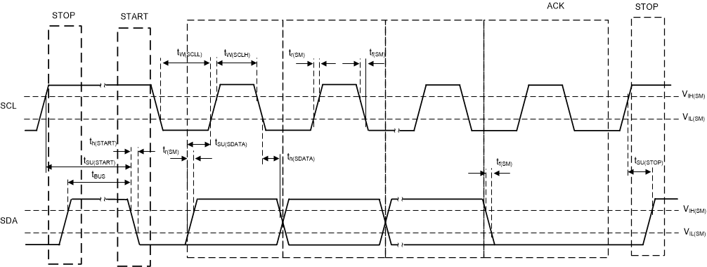
Figure 5-4
I
2
C Timing Diagram
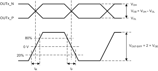
Figure 5-5
Differential Output Voltage and Rise/Fall Time
Figure 5-6
Single-Ended Output Voltage and Rise/Fall Time
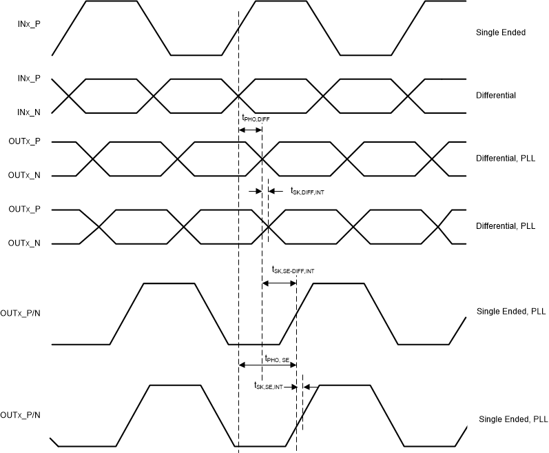
Figure 5-7
Differential and Single-Ended Output Skew and Phase Offset