SNAS805 June 2020 LMK61E08
PRODUCTION DATA.
- 1 Features
- 2 Applications
- 3 Description
- 4 Revision History
- 5 Pin Configuration and Functions
-
6 Specifications
- 6.1 Absolute Maximum Ratings
- 6.2 ESD Ratings
- 6.3 Recommended Operating Conditions
- 6.4 Thermal Information
- 6.5 Electrical Characteristics - Power Supply
- 6.6 LVPECL Output Characteristics
- 6.7 LVDS Output Characteristics
- 6.8 HCSL Output Characteristics
- 6.9 Frequency Tolerance Characteristics
- 6.10 Frequency Margining Characteristics
- 6.11 Power-On Reset Characteristics (VDD)
- 6.12 I2C-Compatible Interface Characteristics (SDA, SCL)
- 6.13 PSRR Characteristics
- 6.14 Other Characteristics
- 6.15 PLL Clock Output Jitter Characteristics
- 6.16 Typical 156.25-MHz Output Phase Noise Characteristics
- 6.17 Typical 161.1328125 MHz Output Phase Noise Characteristics
- 6.18 Additional Reliability and Qualification
- 6.19 Typical Characteristics
- 7 Parameter Measurement Information
-
8 Detailed Description
- 8.1 Overview
- 8.2 Functional Block Diagram
- 8.3
Feature Description
- 8.3.1 Device Block-Level Description
- 8.3.2 Device Configuration Control
- 8.3.3 Register File Reference Convention
- 8.3.4 Configuring the PLL
- 8.3.5 Integrated Oscillator
- 8.3.6 Reference Divider and Doubler
- 8.3.7 Phase Frequency Detector
- 8.3.8 Feedback Divider (N)
- 8.3.9 Fractional Engine
- 8.3.10 Charge Pump
- 8.3.11 Loop Filter
- 8.3.12 VCO Calibration
- 8.3.13 High-Speed Output Divider
- 8.3.14 High-Speed Clock Output
- 8.3.15 Device Status
- 8.4 Device Functional Modes
- 8.5 Programming
- 8.6
Register Maps
- 8.6.1
Register Descriptions
- 8.6.1.1 VNDRID_BY1 Register; R0
- 8.6.1.2 VNDRID_BY0 Register; R1
- 8.6.1.3 PRODID Register; R2
- 8.6.1.4 REVID Register; R3
- 8.6.1.5 SLAVEADR Register; R8
- 8.6.1.6 EEREV Register; R9
- 8.6.1.7 DEV_CTL Register; R10
- 8.6.1.8 XO_CAPCTRL_BY1 Register; R16
- 8.6.1.9 XO_CAPCTRL_BY0 Register; R17
- 8.6.1.10 DIFFCTL Register; R21
- 8.6.1.11 OUTDIV_BY1 Register; R22
- 8.6.1.12 OUTDIV_BY0 Register; R23
- 8.6.1.13 RDIVCMOSCTL Register; R24
- 8.6.1.14 PLL_NDIV_BY1 Register; R25
- 8.6.1.15 PLL_NDIV_BY0 Register; R26
- 8.6.1.16 PLL_FRACNUM_BY2 Register; R27
- 8.6.1.17 PLL_FRACNUM_BY1 Register; R28
- 8.6.1.18 PLL_FRACNUM_BY0 Register; R29
- 8.6.1.19 PLL_FRACDEN_BY2 Register; R30
- 8.6.1.20 PLL_FRACDEN_BY1 Register; R31
- 8.6.1.21 PLL_FRACDEN_BY0 Register; R32
- 8.6.1.22 PLL_MASHCTRL Register; R33
- 8.6.1.23 PLL_CTRL0 Register; R34
- 8.6.1.24 PLL_CTRL1 Register; R35
- 8.6.1.25 PLL_LF_R2 Register; R36
- 8.6.1.26 PLL_LF_C1 Register; R37
- 8.6.1.27 PLL_LF_R3 Register; R38
- 8.6.1.28 PLL_LF_C3 Register; R39
- 8.6.1.29 PLL_CALCTRL Register; R42
- 8.6.1.30 NVMSCRC Register; R47
- 8.6.1.31 NVMCNT Register; R48
- 8.6.1.32 NVMCTL Register; R49
- 8.6.1.33 NVMLCRC Register; R50
- 8.6.1.34 MEMADR Register; R51
- 8.6.1.35 NVMDAT Register; R52
- 8.6.1.36 RAMDAT Register; R53
- 8.6.1.37 NVMUNLK Register; R56
- 8.6.1.38 INT_LIVE Register; R66
- 8.6.1.39 SWRST Register; R72
- 8.6.1
Register Descriptions
- 9 Application and Implementation
- 10Power Supply Recommendations
- 11Layout
- 12Device and Documentation Support
- 13Mechanical, Packaging, and Orderable Information
Package Options
Mechanical Data (Package|Pins)
- SIA|6
Thermal pad, mechanical data (Package|Pins)
Orderable Information
8.5.1 I2C Serial Interface
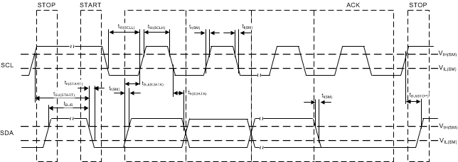
The I2C port on the LMK61E08 works as a slave device and supports both the 100-kHz standard mode and 1-MHz fast mode operations. Fast mode imposes a glitch tolerance requirement on the control signals. Therefore, the input receivers ignore pulses of less than 50-ns duration. The I2C timing is given in I2C-Compatible Interface Characteristics (SDA, SCL). The timing diagram is given in Figure 28.
 Figure 28. I2C Timing Diagram
 In an I2C bus system, the LMK61E08 acts as a slave device and is connected to the serial bus (data bus SDA and lock bus SCL). These are accessed through a 7-bit slave address transmitted as part of an I2C packet. Only the device with a matching slave address responds to subsequent I2C commands. The device slave address is 1011001 or 0x59.
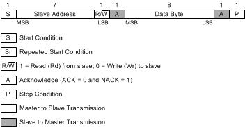
During the data transfer through the I2C interface, one clock pulse is generated for each data bit transferred. The data on the SDA line must be stable during the high period of the clock. The high or low state of the data line can change only when the clock signal on the SCL line is low. The start data transfer condition is characterized by a high-to-low transition on the SDA line while SCL is high. The stop data transfer condition is characterized by a low-to-high transition on the SDA line while SCL is high. The start and stop conditions are always initiated by the master. Every byte on the SDA line must be eight bits long. Each byte must be followed by an acknowledge bit and bytes are sent MSB first. The I2C register structure of the LMK61E08 is shown in Figure 29.
 Figure 29. I2C Register Structure
 The acknowledge bit (A) or non-acknowledge bit (A’) is the 9th bit attached to any 8-bit data byte and is always generated by the receiver to inform the transmitter that the byte has been received (when A = 0) or not (when A’ = 0). A = 0 is done by pulling the SDA line low during the 9th clock pulse and A’ = 0 is done by leaving the SDA line high during the 9th clock pulse.
The I2C master initiates the data transfer by asserting a start condition which initiates a response from all slave devices connected to the serial bus. Based on the 8-bit address byte sent by the master over the SDA line (consisting of the 7-bit slave address (MSB first) and an R/W’ bit), the device whose address corresponds to the transmitted address responds by sending an acknowledge bit. All other devices on the bus remain idle while the selected device waits for data transfer with the master.
After the data transfer has occurred, stop conditions are established. In write mode, the master asserts a stop condition to end data transfer during the 10th clock pulse following the acknowledge bit for the last data byte from the slave. In read mode, the master receives the last data byte from the slave but does not pull SDA low during the 9th clock pulse. This is known as a non-acknowledge bit. By receiving the non-acknowledge bit, the slave knows the data transfer is finished and enters the idle mode. The master then takes the data line low during the low period before the 10th clock pulse, and high during the 10th clock pulse to assert a stop condition. A generic transaction is shown in Figure 30.
 Figure 30. Generic Programming Sequence
 The LMK61E08 I2C interface supports Block Register Write/Read, Read/Write SRAM, and Read/Write EEPROM operations. For Block Register Write/Read operations, the I2C master can individually access addressed registers that are made of an 8-bit data byte.