SNAS826E April   2022  – April 2024 LMK6C , LMK6D , LMK6H , LMK6P

PRODUCTION DATA  

  1.   1
  2. Features
  3. Applications
  4. Description
  5. Device Ordering Information
  6. Pin Configuration and Functions
  7. Specifications
    1. 6.1 Absolute Maximum Ratings
    2. 6.2 ESD Ratings
    3. 6.3 Environmental Compliance
    4. 6.4 Recommended Operating Conditions
    5. 6.5 Thermal Information
    6. 6.6 Thermal Information
    7. 6.7 Electrical Characteristics
    8. 6.8 Timing Diagrams
    9. 6.9 Typical Characteristics
  8. Parameter Measurement Information
    1. 7.1 Device Output Configurations
  9. Detailed Description
    1. 8.1 Overview
    2. 8.2 Functional Block Diagram
    3. 8.3 Feature Description
      1. 8.3.1 Bulk Acoustic Wave (BAW)
      2. 8.3.2 Device Block-Level Description
      3. 8.3.3 Function Pins
      4. 8.3.4 Clock Output Interfacing and Termination
      5. 8.3.5 Temperature Stability
      6. 8.3.6 Mechanical Robustness
    4. 8.4 Device Functional Modes
  10. Application and Implementation
    1. 9.1 Application Information
    2. 9.2 Typical Application
      1. 9.2.1 Design Requirements
      2. 9.2.2 Detailed Design Procedure
      3. 9.2.3 Application Curves
    3. 9.3 Power Supply Recommendations
    4. 9.4 Layout
      1. 9.4.1 Layout Guidelines
        1. 9.4.1.1 Providing Thermal Reliability
        2. 9.4.1.2 Recommended Solder Reflow Profile
      2. 9.4.2 Layout
  11. 10Device and Documentation Support
    1. 10.1 Documentation Support
      1. 10.1.1 Related Documentation
    2. 10.2 Receiving Notification of Documentation Updates
    3. 10.3 Support Resources
    4. 10.4 Trademarks
    5. 10.5 Electrostatic Discharge Caution
    6. 10.6 Glossary
  12. 11Revision History
  13. 12Mechanical, Packaging, and Orderable Information

Package Options

Mechanical Data (Package|Pins)
Thermal pad, mechanical data (Package|Pins)
Orderable Information

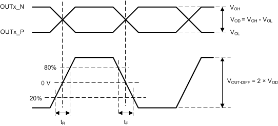
Timing Diagrams

GUID-83DE00F8-285A-41B0-85C5-36BB0F488B03-low.gifFigure 6-1 Differential Output Voltage and Rise/Fall Time
GUID-93BB7238-62BD-490A-AD77-B601408232C2-low.gifFigure 6-2 Single-Ended Output Voltage and Rise/Fall Time