-
LMP2011 Single/LMP2012 Dual High Precision, Rail-to-Rail Output Operational Amplifier
- 1 Features
- 2 Applications
- 3 Description
- 4 Revision History
- 5 Pin Configuration and Functions
-
6 Specifications
- 6.1 Absolute Maximum Ratings
- 6.2 ESD Ratings
- 6.3 Recommended Operating Conditions
- 6.4 Thermal Information: LMP2011
- 6.5 Thermal Information: LMP2012
- 6.6 2.7-V DC Electrical Characteristics
- 6.7 2.7-V AC Electrical Characteristics
- 6.8 5-V DC Electrical Characteristics
- 6.9 5-V AC Electrical Characteristics
- 6.10 Typical Characteristics
- 7 Detailed Description
- 8 Application and Implementation
- 9 Power Supply Recommendations
- 10Layout
- 11Device and Documentation Support
- 12Mechanical, Packaging, and Orderable Information
- IMPORTANT NOTICE
Package Options
Mechanical Data (Package|Pins)
Thermal pad, mechanical data (Package|Pins)
Orderable Information
LMP2011 Single/LMP2012 Dual High Precision, Rail-to-Rail Output Operational Amplifier
1 Features
- Low Ensured VOS Over Temperature 60 µV
- Low Noise with No 1/f 35nV/√Hz
- High CMRR 130 dB
- High PSRR 120 dB
- High AVOL 130 dB
- Wide Gain-Bandwidth Product 3 MHz
- High Slew Rate 4 V/µs
- Low Supply Current 930 µA
- Rail-to-Rail Output 30 mV
- No External Capacitors Required
(For VS = 5 V, Typical Unless Otherwise Noted)
2 Applications
- Precision Instrumentation Amplifiers
- Thermocouple Amplifiers
- Strain Gauge Bridge Amplifier
3 Description
The LMP201x series are the first members of TI's new LMP™ precision amplifier family. The LMP201x series offers unprecedented accuracy and stability in space-saving miniature packaging, offered at an affordable price. This device utilizes patented auto-zero techniques to measure and continually correct the input offset error voltage. The result is an amplifier which is ultra-stable over time and temperature. It has excellent CMRR and PSRR ratings, and does not exhibit the familiar 1/f voltage and current noise increase that plagues traditional amplifiers. The combination of the LMP201x characteristics makes it a good choice for transducer amplifiers, high gain configurations, ADC buffer amplifiers, DAC I-V conversion, and any other 2.7-V to 5-V application requiring precision and long term stability.
Other useful benefits of the LMP201x are rail-to-rail output, a low supply current of 930 µA, and wide gain-bandwidth product of 3 MHz. These versatile features found in the LMP201x provide high performance and ease of use.
Device Information(1)
| PART NUMBER | PACKAGE | BODY SIZE (NOM) |
|---|---|---|
| LMP2011 | SOIC (8) | 4.90 mm × 3.91 mm |
| SOT-23 (5) | 2.90 mm × 1.60 mm | |
| LMP2012 | SOIC (8) | 4.90 mm × 3.91 mm |
| VSSOP (8) | 3.00 mm × 3.00 mm |
- For all available packages, see the orderable addendum at the end of the data sheet.
Bridge Amplifier

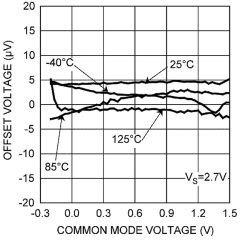
Offset Voltage vs Common Mode Voltage
4 Revision History
Changes from K Revision (March 2013) to L Revision
- Added Pin Configuration and Functions section, Storage Conditions table, ESD Ratings table, Feature Description section, Device Functional Modes, Application and Implementation section, Power Supply Recommendations section, Layout section, Device and Documentation Support section, and Mechanical, Packaging, and Orderable Information section Go
Changes from J Revision (March 2013) to K Revision
- Changed layout of National Data Sheet to TI formatGo
5 Pin Configuration and Functions


Pin Functions: LMP2011
| PIN | I/O | DESCRIPTION | ||||
|---|---|---|---|---|---|---|
| NAME | NO. | |||||
| DBV | D | |||||
| -IN | 4 | 3 | O | Inverting input | ||
| +IN | 3 | 2 | I | Non-Inverting input | ||
| N/C | - | 1 | - | No Internal Connection | ||
| N/C | - | 5 | - | No Internal Connection | ||
| N/C | - | 8 | - | No Internal Connection | ||
| OUT | 1 | 6 | I | Output | ||
| V- | 2 | 4 | P | Negative (lowest) power supply | ||
| V+ | 5 | 7 | P | Positive (highest) power supply | ||

Pin Functions: LMP2012
| PIN | I/O | DESCRIPTION | |||
|---|---|---|---|---|---|
| NAME | NO. | ||||
| D, DGK | |||||
| –IN A | 2 | I | Inverting input, channel A | ||
| +IN A | 3 | I | Non-Inverting input, channel A | ||
| –IN B | 6 | I | Inverting input, channel B | ||
| +IN B | 5 | I | Non-Inverting input, channel B | ||
| OUT A | 1 | O | Output, channel A | ||
| OUT B | 7 | O | Output, channel B | ||
| V– | 4 | P | Negative (lowest) power supply | ||
| V+ | 8 | P | Positive (highest) power supply | ||
6 Specifications
6.1 Absolute Maximum Ratings
See (1)(2)| MIN | MAX | UNIT | ||
|---|---|---|---|---|
| Supply Voltage | 5.8 | V | ||
| Common-Mode Input Voltage | (V-) - 0.3 | (V+) + 0.3 | V | |
| Lead Temperature (soldering 10 sec.) | 300 | °C | ||
| Differential Input Voltage | ±Supply Voltage | |||
| Current at Input Pin | 30 | 30 | mA | |
| Current at Output Pin | 30 | 30 | mA | |
| Current at Power Supply Pin | 50 | 30 | mA | |
| Storage Temperature | −65 | 150 | °C | |
6.2 ESD Ratings
| VALUE | UNIT | |||
|---|---|---|---|---|
| V(ESD) | Electrostatic discharge | Human body model (HBM), per ANSI/ESDA/JEDEC JS-001(1) | ±2000 | V |
| Machine model | ±200 | |||
6.3 Recommended Operating Conditions
| MIN | MAX | UNIT | |
|---|---|---|---|
| Supply Voltage | 2.7 | 5.25 | V |
| Operating Temperature Range | −40 | 125 | °C |
6.4 Thermal Information: LMP2011
| THERMAL METRIC(1) | LMP2011 | UNIT | ||
|---|---|---|---|---|
| D (SOIC) | DBV (SOT-23) | |||
| 8 PINS | 5 PINS | |||
| RθJA | Junction-to-ambient thermal resistance | 119 | 164 | °C/W |
| RθJC(top) | Junction-to-case (top) thermal resistance | 66 | 116 | °C/W |
| RθJB | Junction-to-board thermal resistance | 60 | 28 | °C/W |
| ψJT | Junction-to-top characterization parameter | 17 | 13 | °C/W |
| ψJB | Junction-to-board characterization parameter | 59 | 27 | °C/W |
6.5 Thermal Information: LMP2012
| THERMAL METRIC(1) | LMP2012 | UNIT | ||
|---|---|---|---|---|
| D (SOIC) | DGK (VSSOP) | |||
| 8 PINS | 8 PINS | |||
| RθJA | Junction-to-ambient thermal resistance | 110 | 157 | °C/W |
| RθJC(top) | Junction-to-case (top) thermal resistance | 50 | 51 | °C/W |
| RθJB | Junction-to-board thermal resistance | 52 | 77 | °C/W |
| ψJT | Junction-to-top characterization parameter | 8 | 5 | °C/W |
| ψJB | Junction-to-board characterization parameter | 51 | 75 | °C/W |
6.6 2.7-V DC Electrical Characteristics
Unless otherwise specified, all limits ensured for TJ = 25°C, V+ = 2.7 V, V− = 0 V, V CM = 1.35 V, VO = 1.35 V, and RL > 1 MΩ.| PARAMETER | TEST CONDITIONS | MIN(2) | TYP(1) | MAX(2) | UNIT | ||
|---|---|---|---|---|---|---|---|
| VOS | Input Offset Voltage (LMP2011 only) |
TJ = 25°C | 0.8 | 25 | μV | ||
| The temperature extremes | 60 | ||||||
| Input Offset Voltage (LMP2012 only) |
TJ = 25°C | 0.8 | 36 | ||||
| The temperature extremes | 60 | ||||||
| Offset Calibration Time | TJ = 25°C | 0.5 | 10 | ms | |||
| The temperature extremes | 12 | ||||||
| TCVOS | Input Offset Voltage | 0.015 | μV/°C | ||||
| Long-Term Offset Drift | 0.006 | μV/month | |||||
| Lifetime VOS Drift | 2.5 | μV | |||||
| IIN | Input Current | -3 | pA | ||||
| IOS | Input Offset Current | 6 | pA | ||||
| RIND | Input Differential Resistance | 9 | MΩ | ||||
| CMRR | Common Mode Rejection Ratio | −0.3 ≤ VCM ≤ 0.9 V, 0 ≤ VCM ≤ 0.9 V |
TJ = 25°C | 95 | 130 | dB | |
| The temperature extremes | 90 | ||||||
| PSRR | Power Supply Rejection Ratio | TJ = 25°C | 95 | 120 | dB | ||
| The temperature extremes | 90 | ||||||
| AVOL | Open Loop Voltage Gain | RL = 10 kΩ | TJ = 25°C | 95 | 130 | dB | |
| The temperature extremes | 90 | ||||||
| RL = 2 kΩ | TJ = 25°C | 90 | 124 | ||||
| The temperature extremes | 85 | ||||||
| VO | Output Swing (LMP2011 only) |
RL = 10 kΩ to 1.35 V, VIN(diff) = ±0.5 V |
TJ = 25°C | 2.665 | 2.68 | V | |
| The temperature extremes | 2.655 | ||||||
| TJ = 25°C | 0.033 | 0.060 | |||||
| The temperature extremes | 0.075 | ||||||
| RL = 2 kΩ to 1.35 V, VIN(diff) = ±0.5 V |
TJ = 25°C | 2.630 | 2.65 | V | |||
| The temperature extremes | 2.615 | ||||||
| TJ = 25°C | 0.061 | 0.085 | |||||
| The temperature extremes | 0.105 | ||||||
| Output Swing (LMP2012 only) |
RL = 10 kΩ to 1.35 V, VIN(diff) = ±0.5 V |
TJ = 25°C | 2.64 | 2.68 | V | ||
| The temperature extremes | 2.63 | ||||||
| TJ = 25°C | 0.033 | 0.060 | |||||
| The temperature extremes | 0.075 | ||||||
| RL = 2 kΩ to 1.35 V, VIN(diff) = ±0.5 V |
TJ = 25°C | 2.615 | 2.65 | V | |||
| The temperature extremes | 2.6 | ||||||
| TJ = 25°C | 0.061 | 0.085 | |||||
| The temperature extremes | 0.105 | ||||||
| IO | Output Current | Sourcing, VO = 0 V, VIN(diff) = ±0.5 V |
TJ = 25°C | 5 | 12 | mA | |
| The temperature extremes | 3 | ||||||
| VIN(diff) = ±0.5 V, Sinking, VO = 5 V |
TJ = 25°C | 5 | 18 | ||||
| The temperature extremes | 3 | ||||||
| IS | Supply Current per Channel | TJ = 25°C | 0.919 | 1.20 | mA | ||
| The temperature extremes | 1.50 | ||||||
6.7 2.7-V AC Electrical Characteristics
TJ = 25°C, V+ = 2.7 V, V− = 0 V, VCM = 1.35 V, VO = 1.35 V, and RL > 1 MΩ.| PARAMETER | TEST CONDITIONS | MIN(2) | TYP(1) | MAX(2) | UNIT | ||
|---|---|---|---|---|---|---|---|
| GBW | Gain-Bandwidth Product | 3 | MHz | ||||
| SR | Slew Rate | 4 | V/μs | ||||
| θ m | Phase Margin | 60 | Deg | ||||
| Gm | Gain Margin | −14 | dB | ||||
| en | Input-Referred Voltage Noise | 35 | nV/√Hz | ||||
| enp-p | Input-Referred Voltage Noise | RS = 100 Ω, DC to 10 Hz | 850 | nVpp | |||
| trec | Input Overload Recovery Time | 50 | ms | ||||
6.8 5-V DC Electrical Characteristics
Unless otherwise specified, all limits ensured for TJ = 25°C, V+ = 5 V, V− = 0 V, V CM = 2.5 V, VO = 2.5 V, and RL > 1MΩ.| PARAMETER | TEST CONDITIONS | MIN(2) | TYP(1) | MAX(2) | UNIT | ||
|---|---|---|---|---|---|---|---|
| VOS | Input Offset Voltage (LMP2011 only) |
TJ = 25°C | 0.12 | 25 | μV | ||
| The temperature extremes | 60 | ||||||
| Input Offset Voltage (LMP2012 only) |
TJ = 25°C | 0.12 | 36 | ||||
| The temperature extremes | 60 | ||||||
| Offset Calibration Time | TJ = 25°C | 0.5 | 10 | ms | |||
| The temperature extremes | 12 | ||||||
| TCVOS | Input Offset Voltage | 0.015 | μV/°C | ||||
| Long-Term Offset Drift | 0.006 | μV/month | |||||
| Lifetime VOS Drift | 2.5 | μV | |||||
| IIN | Input Current | -3 | pA | ||||
| IOS | Input Offset Current | 6 | pA | ||||
| RIND | Input Differential Resistance | 9 | MΩ | ||||
| CMRR | Common Mode Rejection Ratio | −0.3 ≤ VCM ≤ 3.2, 0 ≤ VCM ≤ 3.2 |
TJ = 25°C | 100 | 130 | dB | |
| The temperature extremes | 90 | ||||||
| PSRR | Power Supply Rejection Ratio | TJ = 25°C | 95 | 120 | dB | ||
| The temperature extremes | 90 | ||||||
| AVOL | Open Loop Voltage Gain | RL = 10 kΩ | TJ = 25°C | 105 | 130 | dB | |
| The temperature extremes | 100 | ||||||
| RL = 2 kΩ | TJ = 25°C | 95 | 132 | ||||
| The temperature extremes | 90 | ||||||
| VO | Output Swing (LMP2011 only) |
RL = 10 kΩ to 2.5 V, VIN(diff) = ±0.5 V |
TJ = 25°C | 4.96 | 4.978 | V | |
| The temperature extremes | 4.95 | ||||||
| TJ = 25°C | 0.040 | 0.070 | |||||
| The temperature extremes | 0.085 | ||||||
| RL = 2 kΩ to 2.5 V, VIN(diff) = ±0.5 V |
TJ = 25°C | 4.895 | 4.919 | V | |||
| The temperature extremes | 4.875 | ||||||
| TJ = 25°C | 0.091 | 0.115 | |||||
| The temperature extremes | 0.140 | ||||||
| Output Swing (LMP2012 only) |
RL = 10 kΩ to 2.5 V, VIN(diff) = ±0.5 V |
TJ = 25°C | 4.92 | 4.978 | V | ||
| The temperature extremes | 4.91 | ||||||
| TJ = 25°C | 0.040 | 0.080 | |||||
| The temperature extremes | 0.095 | ||||||
| RL = 2 kΩ to 2.5 V, VIN(diff) = ±0.5 V |
TJ = 25°C | 4.875 | 4.919 | V | |||
| The temperature extremes | 4.855 | ||||||
| TJ = 25°C | 0.0.91 | 0.125 | |||||
| The temperature extremes | 0.150 | ||||||
| IO | Output Current | Sourcing, VO = 0 V, VIN(diff) = ±0.5 V |
TJ = 25°C | 8 | 15 | mA | |
| The temperature extremes | 6 | ||||||
| Sinking, VO = 5 V, VIN(diff) = ±0.5 V |
TJ = 25°C | 8 | 17 | ||||
| The temperature extremes | 6 | ||||||
| IS | Supply Current per Channel | TJ = 25°C | 0.930 | 1.20 | mA | ||
| The temperature extremes | 1.50 | ||||||
6.9 5-V AC Electrical Characteristics
TJ = 25°C, V+ = 5 V, V− = 0 V, VCM = 2.5 V, VO = 2.5 V, and RL > 1MΩ.| PARAMETER | TEST CONDITIONS | MIN(2) | TYP(1) | MAX(2) | UNIT | ||
|---|---|---|---|---|---|---|---|
| GBW | Gain-Bandwidth Product | 3 | MHz | ||||
| SR | Slew Rate | 4 | V/μs | ||||
| θ m | Phase Margin | 60 | deg | ||||
| Gm | Gain Margin | −15 | dB | ||||
| en | Input-Referred Voltage Noise | 35 | nV/√Hz | ||||
| enp-p | Input-Referred Voltage Noise | RS = 100 Ω, DC to 10 Hz | 850 | nVpp | |||
| trec | Input Overload Recovery Time | 50 | ms | ||||
6.10 Typical Characteristics
TA=25C, VS= 5 V unless otherwise specified.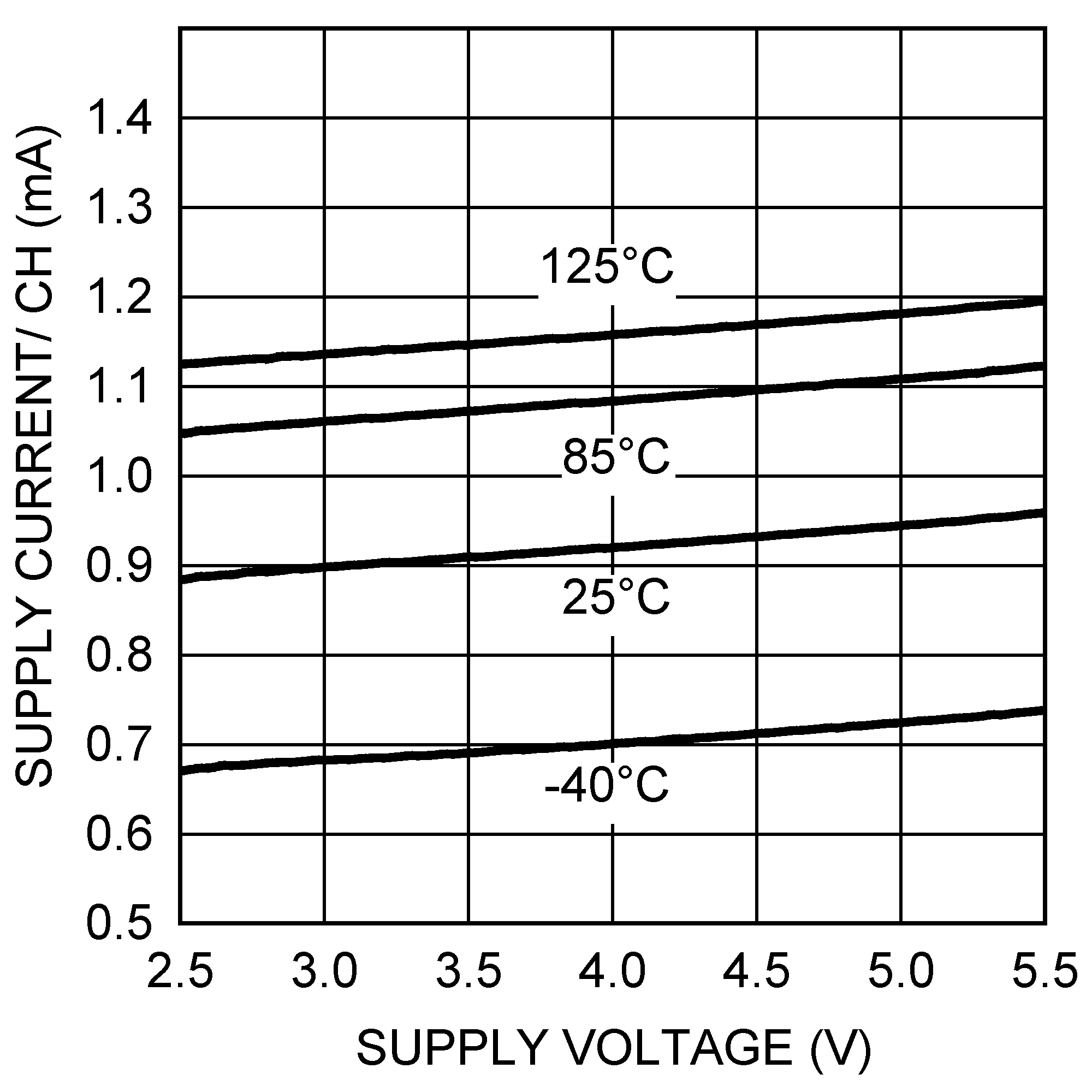 Figure 1. Supply Current vs Supply Voltage
 Figure 3. Offset Voltage vs Common Mode
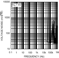 Figure 5. Voltage Noise vs Frequency
 Figure 7. PSRR vs Frequency
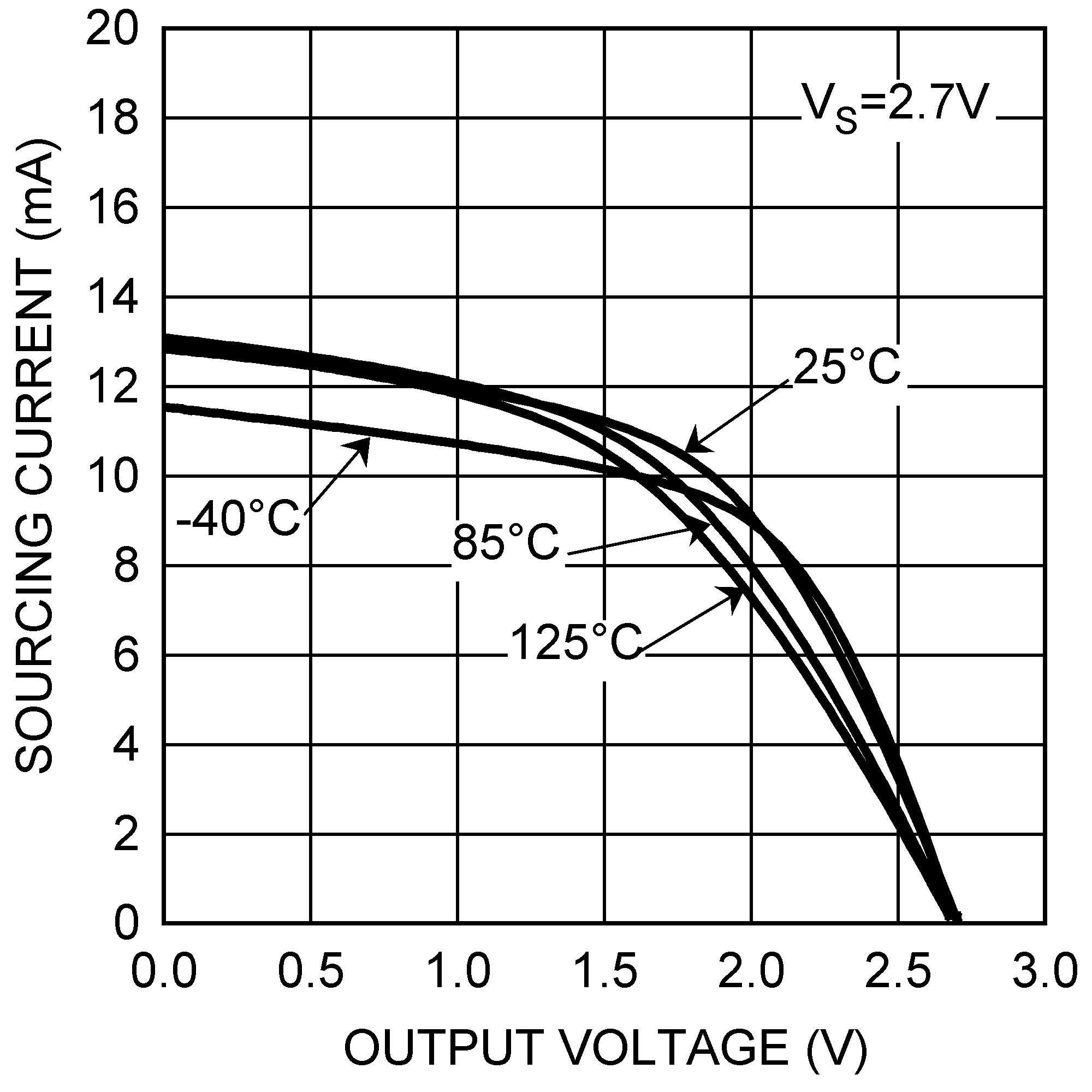 Figure 9. Output Sourcing at 2.7 V
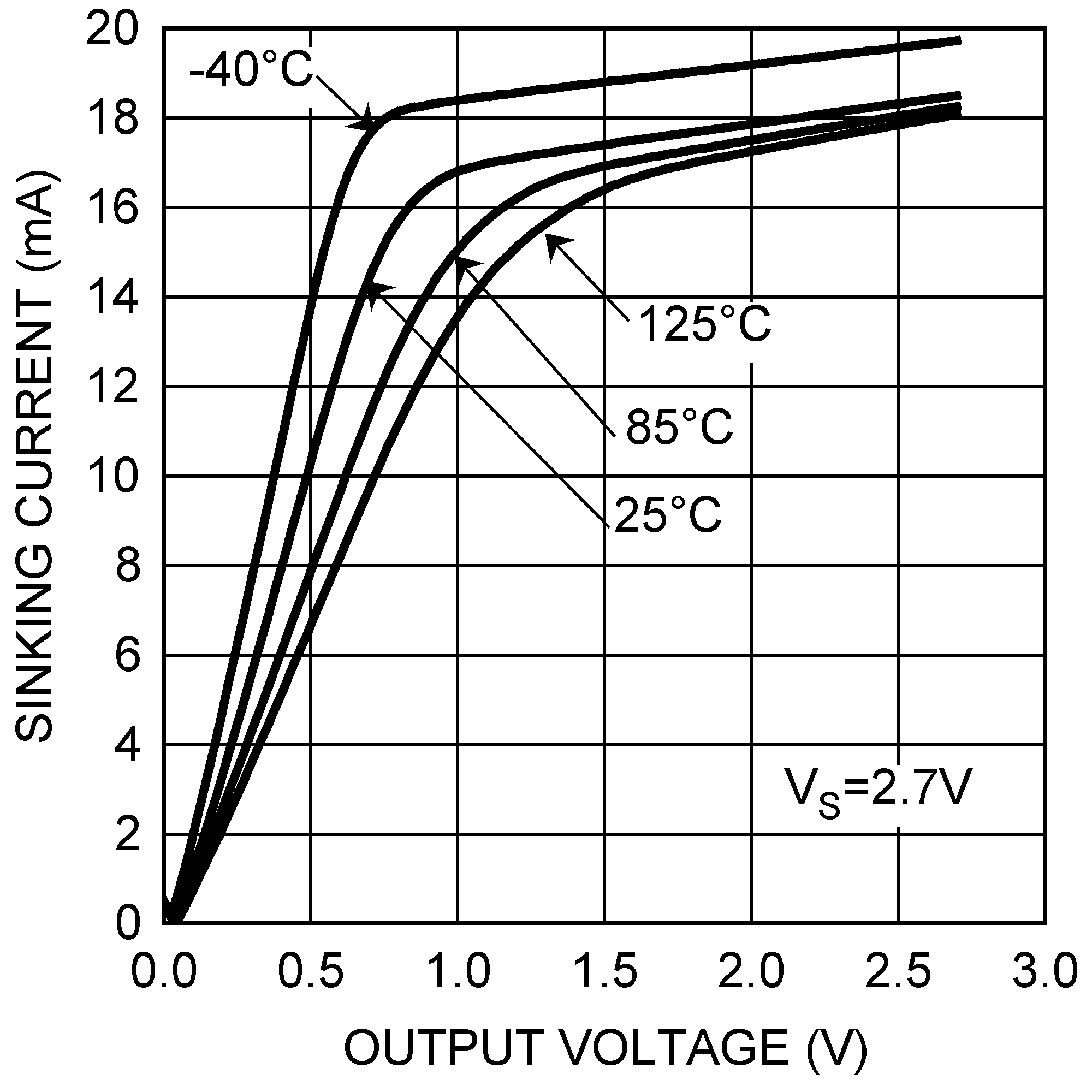 Figure 11. Output Sinking at 2.7 V
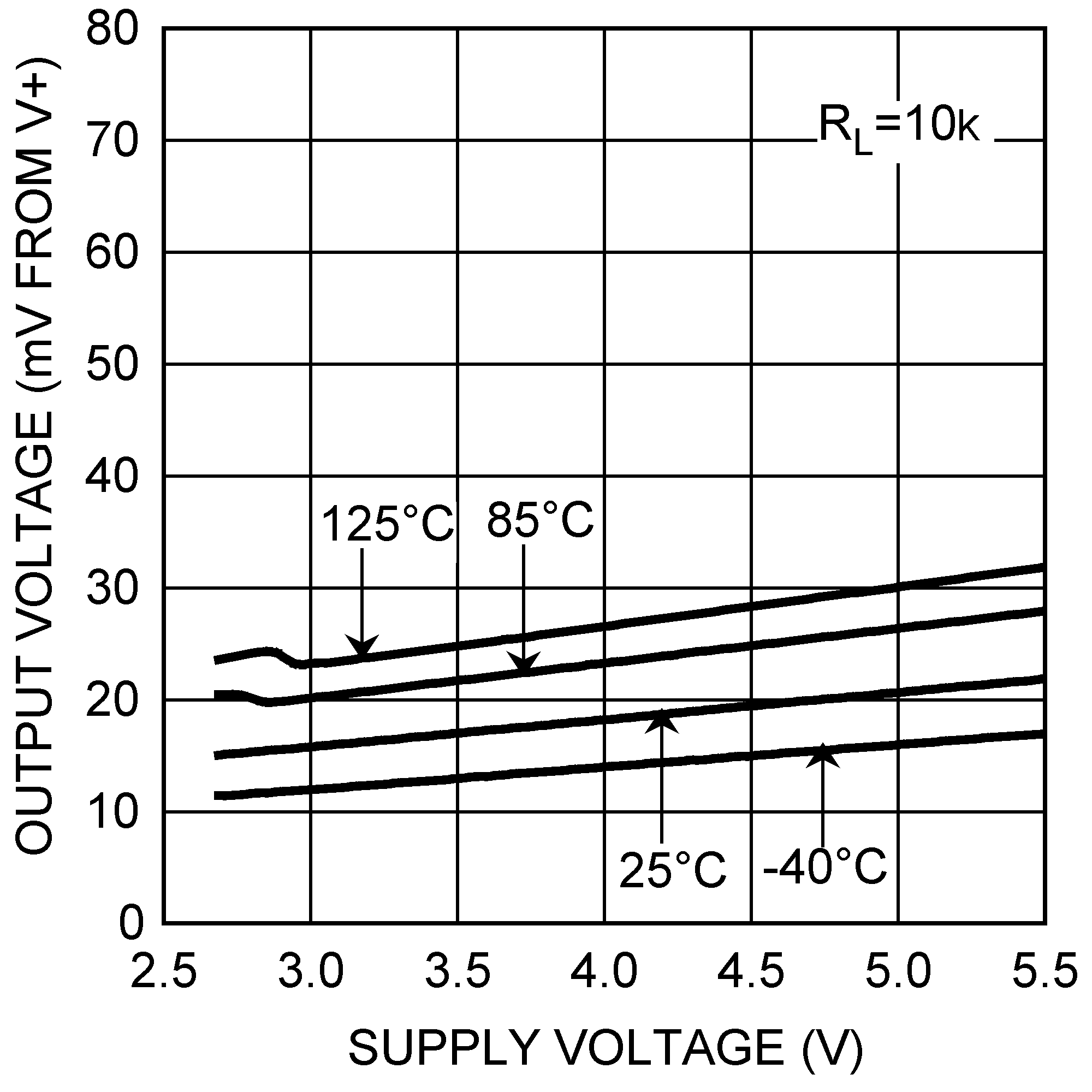 Figure 13. Maximum Output Swing vs Supply Voltage
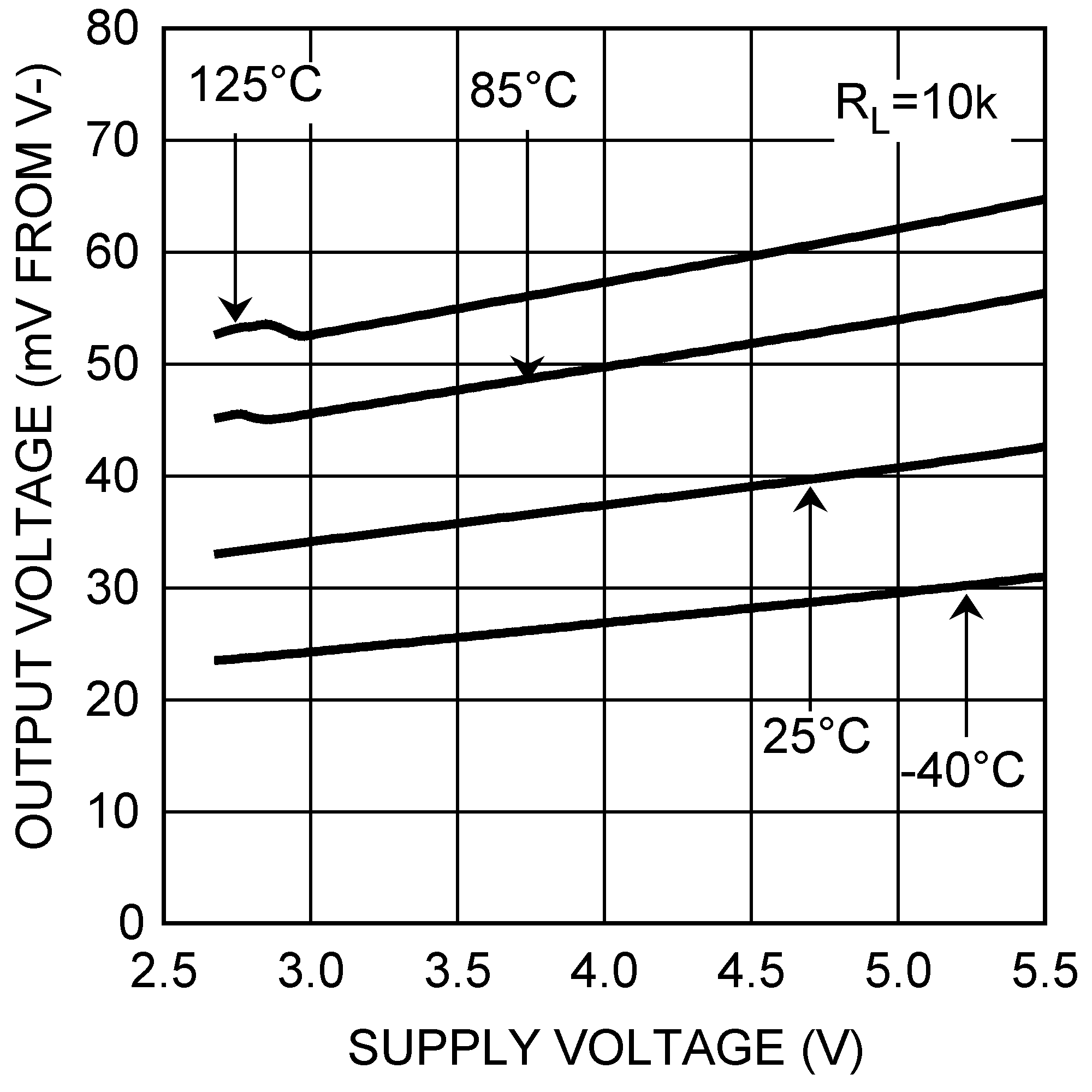 Figure 15. Minimum Output Swing vs Supply Voltage
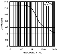 Figure 17. CMRR vs Frequency
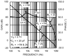 Figure 19. Open Loop Gain and Phase vs RL at 2.7 V
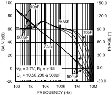 Figure 21. Open Loop Gain and Phase vs CL at 2.7 V
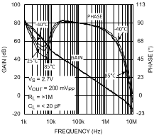 Figure 23. Open Loop Gain and Phase vs Temperature
at 2.7 V
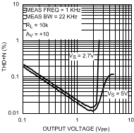 Figure 25. THD+N vs AMPL
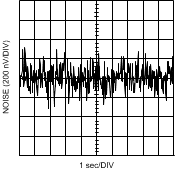 Figure 27. 0.1 Hz − 10 Hz Noise vs Time
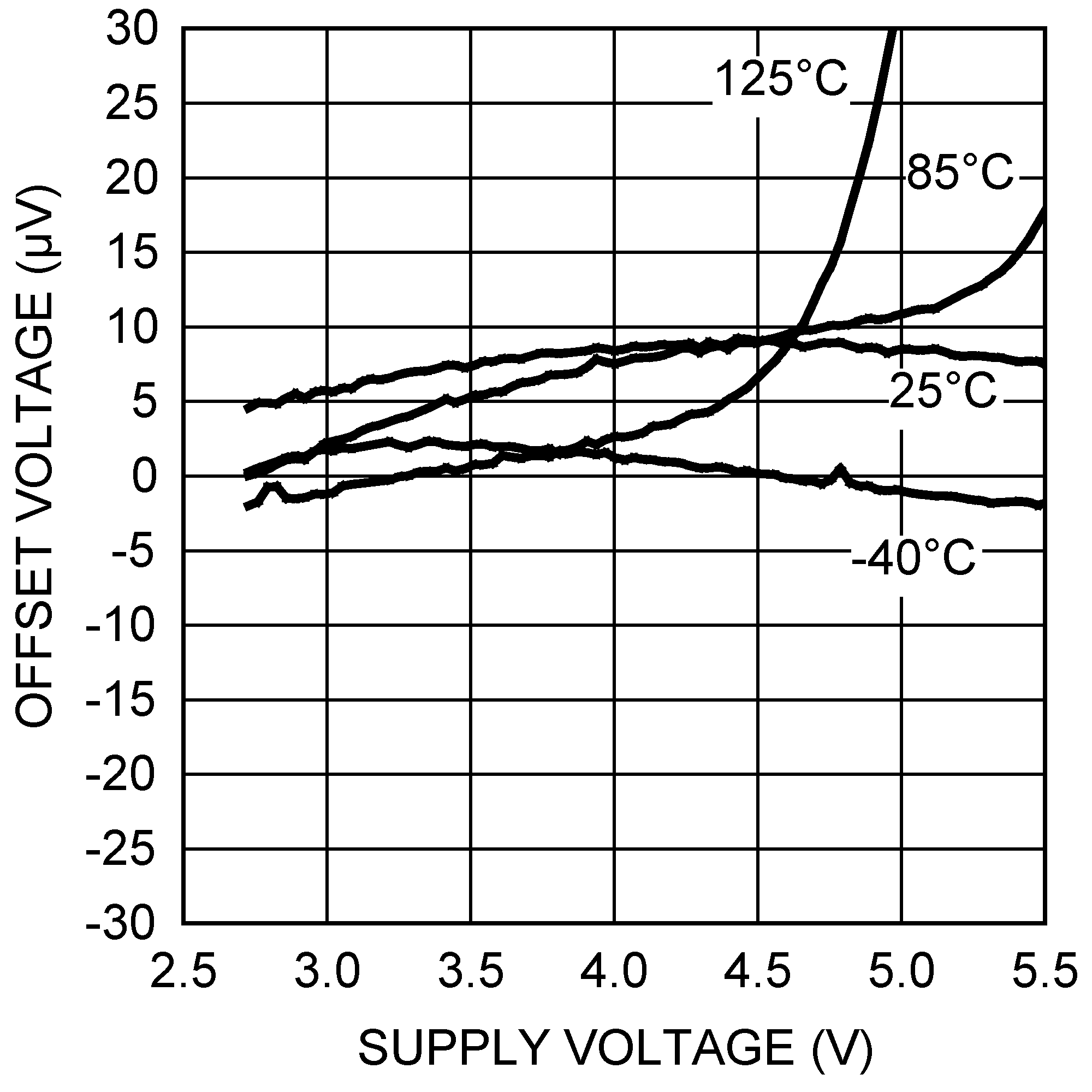 Figure 2. Offset Voltage vs Supply Voltage
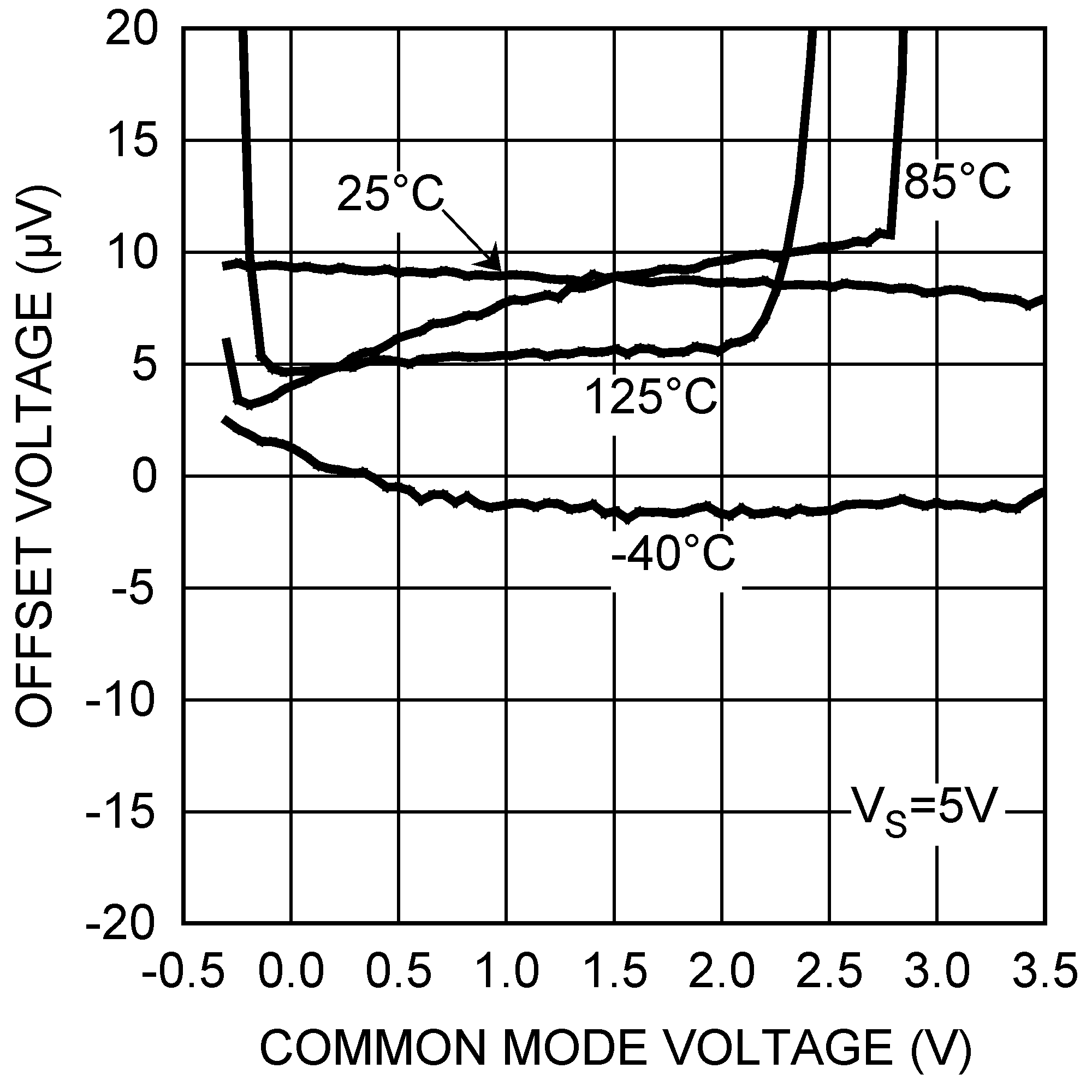 Figure 4. Offset Voltage vs Common Mode
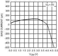 Figure 6. Input Bias Current vs Common Mode
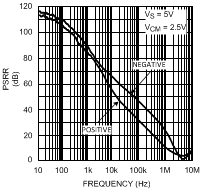 Figure 8. PSRR vs Frequency
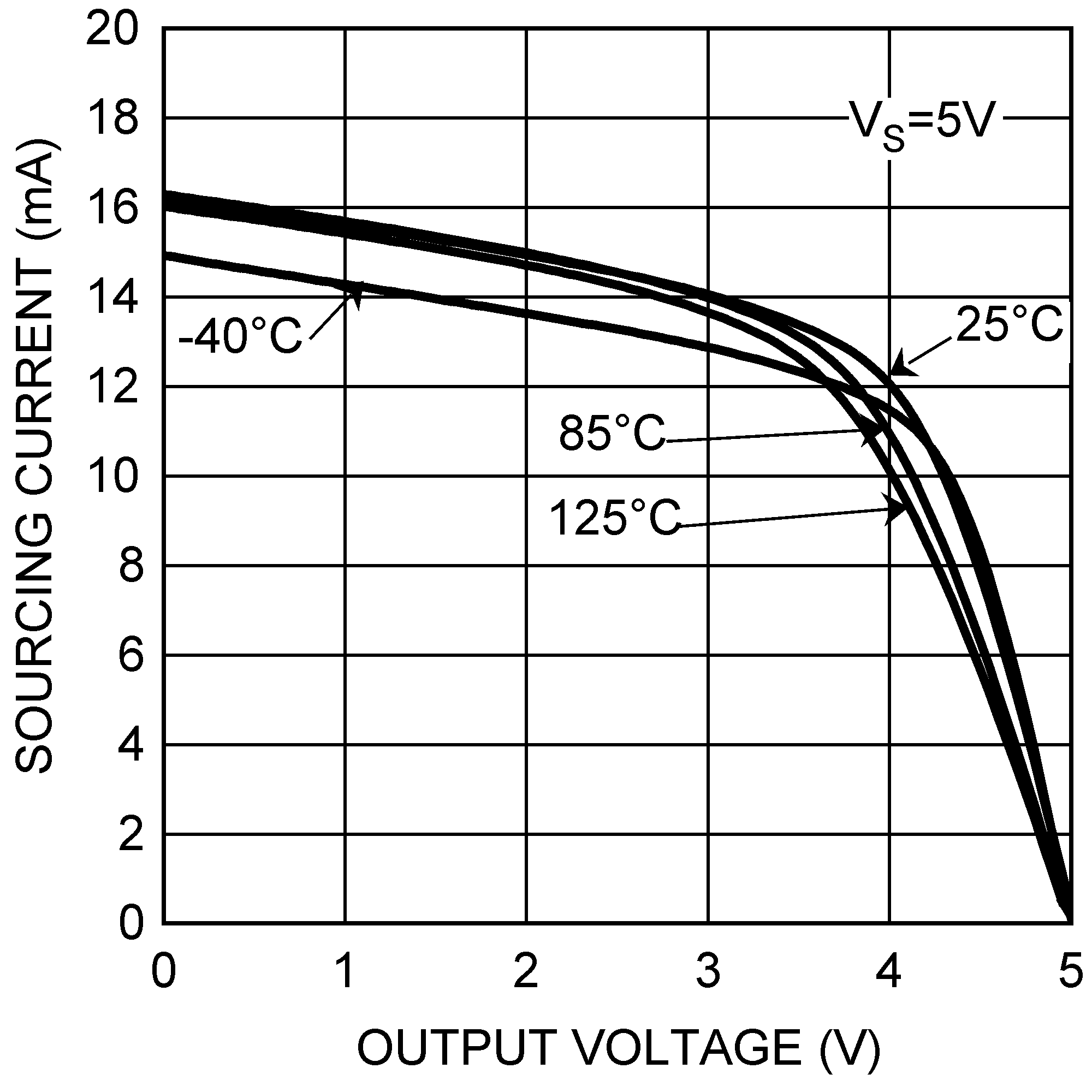 Figure 10. Output Sourcing at 5 V
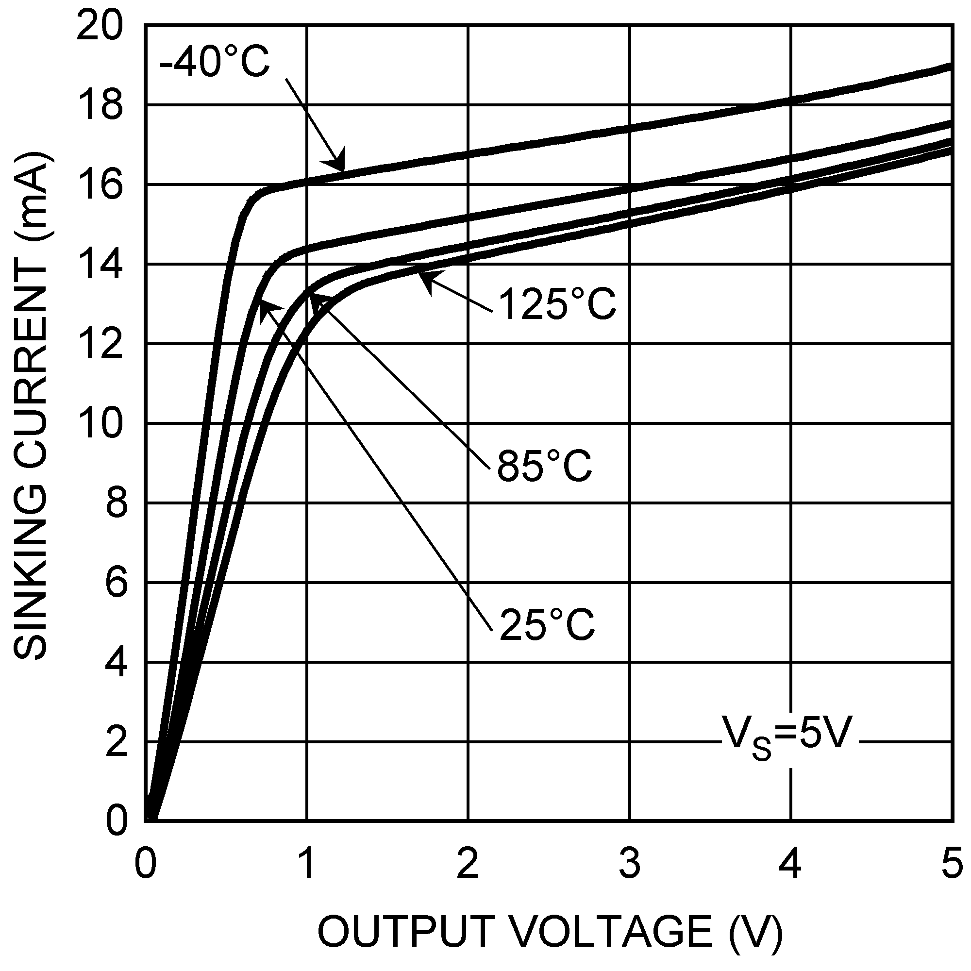 Figure 12. Output Sinking at 5 V
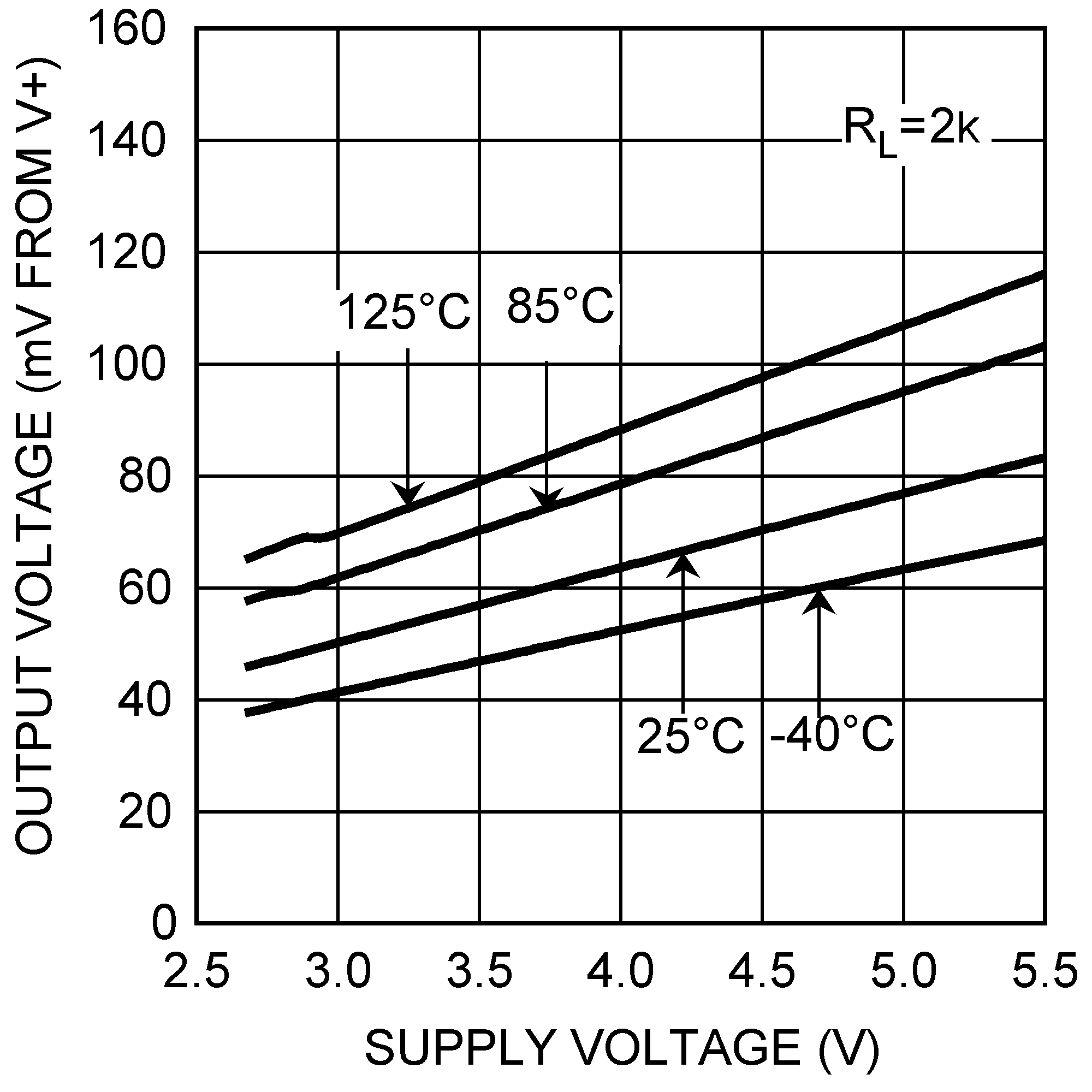 Figure 14. Maximum Output Swing vs Supply Voltage
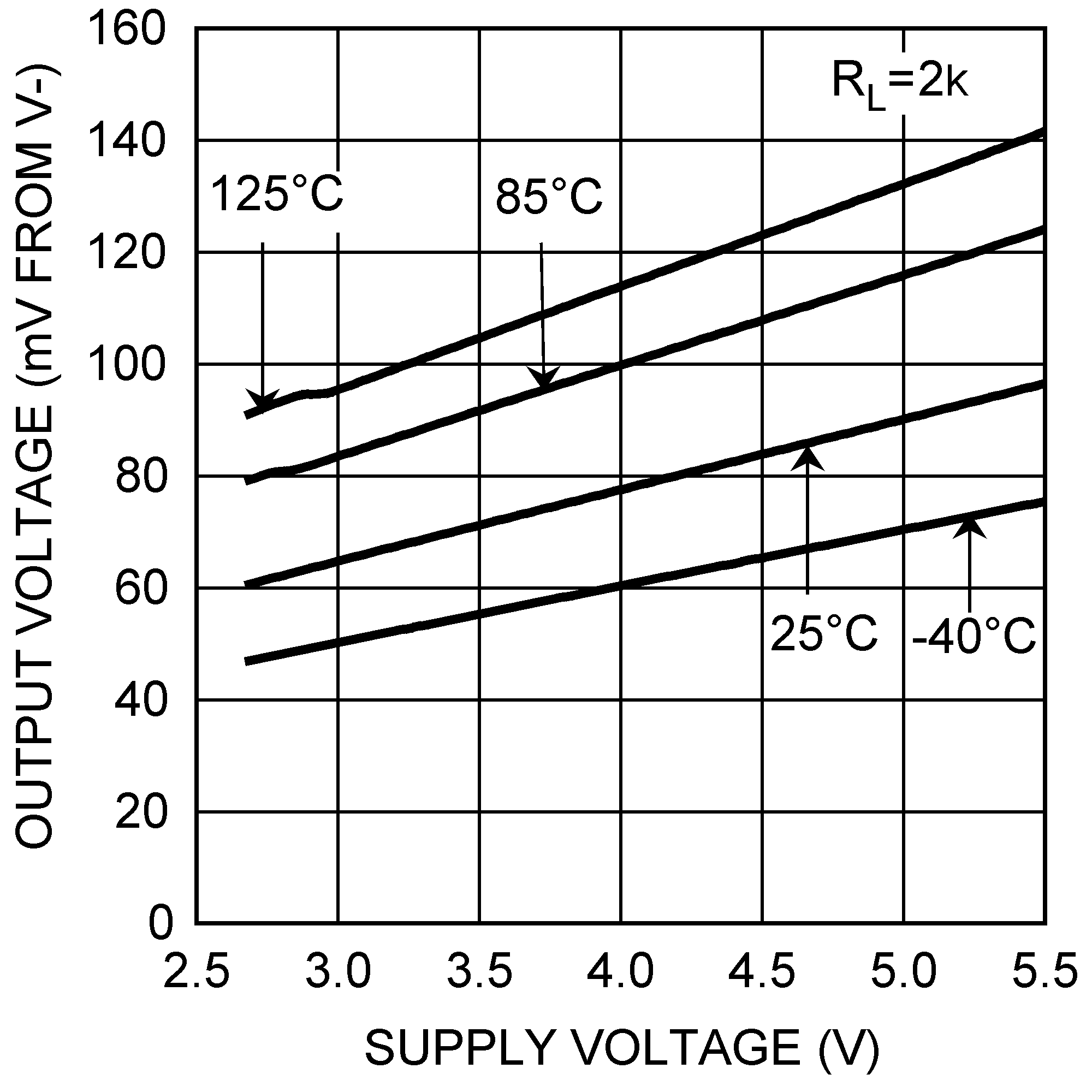 Figure 16. Minimum Output Swing vs Supply Voltage
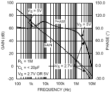 Figure 18. Open Loop Gain and Phase vs Supply Voltage
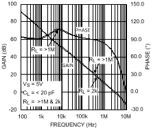 Figure 20. Open Loop Gain and Phase vs RL at 5 V
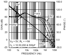 Figure 22. Open Loop Gain and Phase vs CL at 5 V
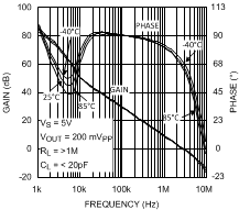 Figure 24. Open Loop Gain and Phase vs Temperature
at 5 V
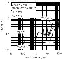 Figure 26. THD+N vs Frequency