SNOSAY9G September 2008 – February 2016 LMP2021 , LMP2022
PRODUCTION DATA.
- 1 Features
- 2 Applications
- 3 Description
- 4 Revision History
- 5 Pin Configuration and Functions SC-70 and VSSOP references from LMP2021 pinout descriptions
- 6 Specifications
- 7 Detailed Description
- 8 Application and Implementation
- 9 Power Supply Recommendations
- 10Layout
- 11Device and Documentation Support
- 12Mechanical, Packaging, and Orderable Information
Package Options
Mechanical Data (Package|Pins)
Thermal pad, mechanical data (Package|Pins)
Orderable Information
8 Application and Implementation
NOTE
Information in the following applications sections is not part of the TI component specification, and TI does not warrant its accuracy or completeness. TI’s customers are responsible for determining suitability of components for their purposes. Customers should validate and test their design implementation to confirm system functionality.
8.1 Application Information
8.1.1 Achieving Lower Noise With Filtering
The low input voltage noise of the LMP202x, and no 1/f noise make these suitable for many applications with noise sensitive designs. Simple filtering can be done on the LMP202x to remove high frequency noise. Figure 37 shows a simple circuit that achieves this.
In Figure 37 CF and the corner frequency of the filter resulting from CF and RF will reduce the total noise.
 Figure 37. Noise Reducing Filter for Lower Gains
In order to achieve lower noise floors for even more noise stringent applications, a simple filter can be added to the op amp’s output after the amplification stage. Figure 38 shows the schematic of a simple circuit which achieves this objective. Low noise amplifiers such as the LMV771 can be used to create a single pole low pass filter on the output of the LMP202x. The noise performance of the filtering amplifier, LMV771 in this circuit, will not be dominant as the input signal on LMP202x has already been significantly gained up and as a result the effect of the input voltage noise of the LMV771 is effectively not noticeable.
 Figure 38. Enhanced Filter to Further Reduce Noise at Higher Gains
Using the circuit in Figure 38 has the advantage of removing the non-linear filter bandwidth dependency which is seen when the circuit in Figure 37 is used. The difference in noise performance of the circuits in Figure 37 and Figure 38 becomes apparent only at higher gains. At voltage gains of 10 V/V or less, there is no difference between the noise performance of the two circuits.
 Figure 39. RMS Input Referred Noise vs. Frequency
Figure 39 shows the total input referred noise vs. 3 dB corner of both filters of Figure 37 and Figure 38 at gains of 100V/V and 1000V/V. For these measurements and using Figure 37's circuit, RF = 49.7 kΩ and RIN = 497Ω. Value of CF has been changed to achieve the desired 3 dB filter corner frequency. In the case of Figure 38's circuit, RF = 49.7 kΩ and RIN = 497Ω, RFILT = 49.7 kΩ, and CFILT has been changed to achieve the desired 3 dB filter corner frequency. Figure 39 compares the RMS noise of these two circuits. As Figure 39 shows, the RMS noise measured the circuit in Figure 38 has lower values and also depicts a more linear shape.
8.1.2 Input Bias Current
The bias current of the LMP202x behaves differently than a conventional amplifier due to the dynamic transient currents created on the input of an auto-zero circuit. The input bias current is affected by the charge and discharge current of the input auto-zero circuit. This effectivly creates a repetitive impulse current noise of 100's of pA. For this reason, the LMP202x is not recommeded for source impedances of 1 MΩ or greater.
The amount of current sunk or sourced from that stage is dependent on the combination of input impedance (resistance and capacitance), as well as the balance and matching of these impedances across the two inputs. This current, integrated by the input capacitence, causes a shift in the apparent "bias current". Because of this, there is an apparent "bias current vs. input impedance" interaction. In the LMP202x for an input resistive impedance of 1 GΩ, the shift in input bias current can be up to 40 pA. This input bias shift is caused by varying the input's capacitive impedance. Since the input bias current is dependent on the input impedance, it is difficult to estimate what the actual bias current is without knowing the end circuit and associated capacitive strays.
Figure 40 shows the input bias current of the LMP202x and that of another commercially available amplifier from a competitor. As it can be seen, the shift in LMP202x bias current is much lower than that of other chopper style or auto zero amplifiers available from other vendors.
 Figure 40. Input Bias Current of LMP202x is lower than Competitor A
8.1.3 Lowering the Input Bias Current
As mentioned in the Input Bias Current section, the input bias current of an auto zero amplifier such as the LMP202x varies with input impedance and feedback impedance. Once the value of a certain input resistance, i.e. sensor resistance, is known, it is possible to optimize the input bias current for this fixed input resistance by choosing the capacitance value that minimizes that current. Figure 41 shows the input bias current vs. input impedance of the LMP202x. The value of RG or input resistance in this test is 1 GΩ. When this value of input resistance is used, and when a parallel capacitance of 22 pF is placed on the circuit, the resulting input bias current is nearly 0 pA. Figure 41 can be used to extrapolate capacitor values for other sensor resistances. For this purpose, the total impedance seen by the input of the LMP202x needs to be calculated based on Figure 41. By knowing the value of RG, one can calculate the corresponding CG which minimizes the non-inverting input bias current, positive bias current, value.
 Figure 41. Input Bias Current vs. CG with RG = 1 GΩ
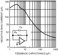
In a typical I-V converter, the output voltage will be the sum of DC offset plus bias current and the applied signal through the feedback resistor. In a conventional input stage, the inverting input's capacitance has very little effect on the circuit. This effect is generally on settling time and the dielectric soakage time and can be ignored. In auto zero amplifiers, the input capacitance effect will add another term to the output. This additional term means that the baseline reading on the output will be dependent on the input capacitance. The term input capacitance for this purpose includes circuit strays and any input cable capacitances. There is a slight variation in the capacitive offset as the duty cycle and amplitude of the pulses vary from part to part, depending on the correction at the time. The lowest input current will be obtained when the impedances, both resistive and capacitive, are matched between the inputs. By balancing the input capacitances, the effect can be minimized. A simple way to balance the input impedance is adding a capacitance in parallel to the feedback resistance. The addition of this feedback capacitance reduces the bias current and increases the stability of the operational amplifier. Figure 42 shows the input bias current of the LMP202x when RF is set to 1 GΩ. As it can be seen from Figure 42, choosing the optimum value of CF will help reducing the input bias current.
 Figure 42. Input Bias Current vs. CF with RF = 1 GΩ
The effect of bias current on a circuit can be estimated with the following:
Where AV is the closed loop gain of the system and IBIAS+ and IBIAS− denote the positive and negative bias current, respectively. It is common to show the average of these bias currents in product datasheets. If IBIAS+ and IBIAS− are not individually specified, use the IBIAS value provided in datasheet graphs or tables for this calculation.
For the application circuit shown in Figure 46, the LMP2022 amplifiers each have a gain of 18. With a sensor impedance of 500Ω for the bridge, and using the above equation, the total error due to the bias current on the outputs of the LMP2022 amplifier will be less than 200 nV.
8.1.4 Sensor Impedance
The sensor resistance, or the resistance connected to the inputs of the LMP202x, contributes to the total impedance seen by the auto correcting input stage.

 Figure 43. Auto Correcting Input Stage Model
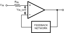
As shown in Figure 43, the sum of RIN and RON-SWITCH will form a low pass filter with COUT during correction cycles. As RIN increases, the time constant of this filter increases, resulting in a slower output signal which could have the effect of reducing the open loop gain, AVOL, of the LMP202x. In order to prevent this reduction in AVOL in presence of high impedance sensors or other high resistances connected to the input of the LMP202x, a capacitor can be placed in parallel to this input resistance. This is shown in Figure 44.

 Figure 44. Sensor Impedance with Parallel Capacitance
CIN in Figure 44 adds a zero to the low pass filter and hence eliminating the reduction in AVOL of the LMP202x. An alternative circuit to achieve this is shown in Figure 45.
 Figure 45. Alternative Sensor Impedance Circuit
8.1.5 Transient Response to Fast Inputs
On chip continuous auto zero correction circuitry eliminates the 1/f noise and significantly reduces the offset voltage and offset voltage drift; all of which are very low frequency events. For slow changing sensor signals this correction is transparent. For excitations which may otherwise cause the output to swing faster than 40 mV/µs, there are additional considerations which can be viewed two perspectives: for sine waves and for steps.
For sinusoidal inputs, when the output is swinging rail-to-rail on ±2.5-V supplies, the auto zero circuitry will introduce distortions above 2.55 kHz. For smaller output swings, higher frequencies can be amplified without the auto zero slew limitation as shown in table below. Signals above 20 kHz, are not affected, though normally, closed loop bandwidth should be kept below 20 kHz so as to avoid aliasing from the auto zero circuit.
| VOUT-PEAK (V) | fMAX-SINE WAVE (kHz) |
|---|---|
| 0.32 | 20 |
| 1 | 6.3 |
| 2.5 | 2.5 |
For step-like inputs, such as those arising from disturbances to a sensing system, the auto zero slew rate limitation manifests itself as an extended ramping and settling time, lasting ~100 µs.
8.1.6 Digital Acquisition Systems
High resolution ADC’s with 16-bits to 24-bits of resolution can be limited by the noise of the amplifier driving them. The circuit configuration, the value of the resistors used and the source impedance seen by the amplifier can affect the noise of the amplifier. The total noise at the output of the amplifier can be dominated by one of several sources of noises such as: white noise or broad band noise, 1/f noise, thermal noise, and current noise. In low frequency applications such as medical instrumentation, the source impedance is generally low enough that the current noise coupled into it does not impact the total noise significantly. However, as the 1/f or flicker noise is paramount to many application, the use of an auto correcting stabilized amplifier like the LMP202x reduces the total noise.
Table 1 summarizes the input and output referred RMS noise values for the LMP202x compared to that of Competitor A. As described in previous sections, the outstanding noise performance of the LMP202x can be even further improved by adding a simple low pass filter following the amplification stage.
The use of an additional filter, as shown in Figure 38 benefits applications with higher gain. For this reason, at a gain of 10, only the results of circuit in Figure 37 are shown. The RMS input noise of the LMP202x are compared with Competitor A's input noise performance. Competitor A's RMS input noise behaves the same with or without an additional filter.
Table 1. RMS Input Noise Performance
| Amplifier Gain (V/V) |
System Bandwidth Requirement (Hz) | RMS Input Noise (nV) | |||
|---|---|---|---|---|---|
| LMP202x | Competitor A | ||||
| Figure 37 Circuit | Figure 38 Circuit | Figure 37, Figure 38 Circuit | |||
| 10 | 100 | 229 | See(1) | 300 | |
| 1000 | 763 | See(1) | 1030 | ||
| 100 | 100 | 229 | 196 | 300 | |
| 1000 | 763 | 621 | 1030 | ||
| 1000 | 10 | 71 | 46 | 95 | |
| 100 | 158 | 146 | 300 | ||
| 1000 | 608 | 462 | 1030 | ||
8.2 Typical Application
Figure 46 shows the Bridge Sensor Interface for these devices.
8.2.1 Design Requirements
Bridge sensors are used in a variety of applications such as pressure sensors and weigh scales. Bridge sensors typically have a very small differential output signal. This very small differential signal needs to be accurately amplified before it can be fed into an ADC. As discussed in the previous sections, the accuracy of the op amp used as the ADC driver is essential to maintaining total system accuracy.
The high DC performance of the LMP202x make these amplifiers ideal choices for use with a bridge sensor. The LMP202x have very low input offset voltage and very low input offset voltage drift. The open loop gain of the LMP202x is 160 dB.
The circuit in Figure 46 shows a signal path solution for a typical bridge sensor using the LMP202x. Bridge sensors are created by replacing at least one of the resistors in a typical bridge with a sensor whose resistance varies in response to an external stimulus. For this example, the expected bridge output signal will be in the range of ±12 mV. This signal must be accurately amplified by the amplifier to best match the dynamic input range of the ADC. This is done by using one LMP2022 and one LMP2021 in front of the ADC161S626.
The on chip EMI rejection filters available on the LMP202x help remove the EMI interference introduced to the signal and hence improve the overall system performance.
8.2.2 Detailed Design Procedure
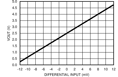
The amplification of this ±12 mV signal is achieved in 2 stages and through a three op-amp instrumentation amplifier. The dual LMP2022 in Figure 46 amplifies each side of the differential output of the bridge sensor by a gain of 18.2. Using the LMP2022 with a gain of 18.2 reduces the input referred voltage noise of the op amps and the system as a result. Also, this gain allows direct filtering of the signal on the LMP2022 without compromising noise performance. The differential output of the two amplifiers in the LMP2022 are then fed into a LMP2021 configured as a difference amplifier. This stage has a gain of 5, with a total system having a gain of (18.2 * 2 +1 ) * 5 = 187. The LMP2021 has an outstanding CMRR value of 139. This impressive CMRR improves system performance by removing the common mode signal introduced by the bridge. With an overall gain of 187, the ±12 mV differential input signal is gained up to ±2.24V (0.26 V to 4.74V single ended). This utilizes the amplifiers output swing as well as the ADC's input dynamic range, and allows for some overload range.
Bridge sensor measurements are usually done up to 10s of Hz. Placing a 300 Hz filter on the LMP2022 helps removing the higher frequency noise from this circuit. This filter is created by placing two capacitors in the feedback path of the LMP2022 amplifiers.
This amplified signal is then fed into the ADC161S626. The ADC161S626 is a 16-bit, 50 kSPS to 250 kSPS 5V ADC. In order to utilize the maximum number of bits of the ADC161S626 in this configuration, a 2.5V reference voltage is used. This 2.5V reference is also used to power the bridge sensor and the inverting input of the ADC. Using the same voltage source for these three points helps reducing the total system error by eliminating error due to source variations.
With this system, the output signal of the bridge sensor which can be up to ±13.3 mV and is accurately scaled to the full scale range of the ADC and then digitized for further processing. The LMP202x introduced minimal error to the system and improved the signal quality by removing common mode signals and high frequency noise.
8.2.3 Application Curve
 Figure 47. Single Ended Output Results for Bridge Circuit
