SNOSDB6D December 2020 – October 2024 LMP7704-SP
PRODUCTION DATA
- 1
- 1 Features
- 2 Applications
- 3 Description
- 4 Pin Configuration and Functions
- 5 Specifications
- 6 Detailed Description
- 7 Application and Implementation
- 8 Device and Documentation Support
- 9 Revision History
- 10Mechanical, Packaging, and Orderable Information
Package Options
Refer to the PDF data sheet for device specific package drawings
Mechanical Data (Package|Pins)
- HBH|14
Thermal pad, mechanical data (Package|Pins)
Orderable Information
7.2.2 Detailed Design Procedure
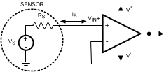
Many sensors have high source impedances that can range up to 10 MΩ. The output signal of sensors must often be amplified or otherwise conditioned by means of an amplifier. The input bias current of this amplifier can load the sensor output and cause a voltage drop across the source resistance, shown in Figure 7-4, where VIN+ = VS – IBIAS × RS.
 Figure 7-4 Offset Error
Due to IBIAS
Figure 7-4 Offset Error
Due to IBIASThe last term, IBIAS * RS, shows the voltage drop across RS. To prevent errors introduced to the system due to this voltage, an op amp with very low input bias current must be used with high impedance sensors. An amplifier with low input bias also has low input current noise, further improving the accuracy of systems with high source resistance.
Figure 7-3 shows one channel of the LMP7704-SP configured for a gain of 25. A high source impedance is placed between the input signal and the noninverting input of the amplifier to represent the output impedance of the sensor.
With the ultra-low input bias current of the LMP7704-SP, even with a signal source that has high output impedance, the system output maintains very good linearity to the ideal output voltage (that is, the output of an ideal amplifier in the same configuration). Figure 7-5 shows the output voltage vs input voltage of the LMP7704-SP with a 10-MΩ source impedance. Figure 7-6 shows the output voltage vs input voltage for an ideal amplifier with no input bias current. Comparing the two graphs shows that the LMP7704-SP maintains high accuracy even with a large source impedance connected to an input.