SNVS829E March 1999 – February 2017 LMP8480 , LMP8481
PRODUCTION DATA.
- 1 Features
- 2 Applications
- 3 Description
- 4 Revision History
- 5 Device Comparison Table
- 6 Pin Configuration and Functions
- 7 Specifications
-
8 Detailed Description
- 8.1 Overview
- 8.2 Functional Block Diagrams
- 8.3
Feature Description
- 8.3.1 Basic Connections
- 8.3.2 Selection of the Sense Resistor
- 8.3.3 Using PCB Traces as Sense Resistors
- 8.3.4 VREFA and VREFB Pins (LMP8481 Only)
- 8.3.5 Reference Input Voltage Limits (LMP8481 Only)
- 8.3.6 Low-Side Current Sensing
- 8.3.7 Input Series Resistance
- 8.3.8 Minimum Output Voltage
- 8.3.9 Swinging Output Below Ground
- 8.3.10 Maximum Output Voltage
- 8.4 Device Functional Modes
- 9 Application and Implementation
- 10Power Supply Recommendations
- 11Layout
- 12Device and Documentation Support
- 13Mechanical, Packaging, and Orderable Information
Package Options
Mechanical Data (Package|Pins)
- DGK|8
Thermal pad, mechanical data (Package|Pins)
Orderable Information
9 Application and Implementation
NOTE
Information in the following applications sections is not part of the TI component specification, and TI does not warrant its accuracy or completeness. TI’s customers are responsible for determining suitability of components for their purposes. Customers should validate and test their design implementation to confirm system functionality.
9.1 Application Information
The LMP848x amplifies the voltage developed across a current-sensing resistor when current passes through it. Flexible offset inputs allow adjusting the functionality of the output for multiple configurations, as discussed throughout this section.
9.1.1 Input Common-Mode and Differential Voltage Range
The input common-mode range, where common-mode range is defined as the voltage from ground to the voltage on RSP input, must be in the range of 4.0 V to 76 V. Operation below 4.0 V on either input pin introduces severe gain error and nonlinearities.
The maximum differential voltage (defined as the voltage difference between RSP and RSN) must be 667 mV or less. The theoretical maximum input is 700 mV (14 V / 20).
Taking the inputs below 4 V does not damage the device, but the output conditions during this time are not predictable and are not ensured.
If the load voltage (Vcm) is expected to fall below 4 V as part of normal operation, preparations must be made for invalid output levels during this time.
9.2 Typical Applications
9.2.1 Unidirectional Application With the LMP8480
 Figure 27. Unidirectional Application with the LMP8480
9.2.1.1 Design Requirements
The LMP8480 is designed for unidirectional current sense applications. The output of the amplifier is equal to the differential input voltage times the fixed device gain.
9.2.1.2 Detailed Design Procedure
The output voltage can be calculated from Equation 9:
Note that the minimum zero reading is limited by the lower output swing and input offset. The LMP8480 is functionally identical to the LMP8481, but with the VREFA and VREFB nodes grounded internally. The LMP8481 can replace the LMP8480 if both the VREF inputs (pins 6 and 7) are grounded.
9.2.1.3 Application Curve
 Figure 28. Unidirectional Transfer Function for Gain-of-20 Option
9.2.2 Bidirectional Current Sensing Using the LMP8481
 Figure 29. Bidirectional Current Sensing Using the LMP8481
9.2.2.1 Design Requirements
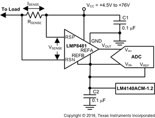
Bidirectional operation is required where the measured load current can be positive or negative. Because VSENSE can be positive or negative, and the output cannot swing negative, the zero output level must be level-shifted above ground to a known zero reference point. The LMP8481 allows for the setting this reference point.
9.2.2.2 Detailed Design Procedure
The VREFA and VREFB pins set the zero reference point. The output zero reference point is set by applying a voltage to the REFA and REFB pins; see the Unidirectional Application With the LMP8480 section. The VREFA and VREFB Pins (LMP8481 Only) section describes the output transfer function with a 1.2-V reference applied to the gain-of-20 option.
9.2.2.3 Application Curve
 Figure 30. Bidirectional Transfer Function Using a 1.2-V Reference Voltage
9.2.3 Typical Application With a Resistive Divider
Take care if the output is driving an A/D input with a maximum A/D maximum input voltage lower than the amplifier supply voltage because the output can swing higher than the planned load maximum resulting from input transients or shorts on the load and overload or possibly damage the A/D input.
A resistive attenuator, as shown in Figure 31, can be used to match the maximum swing to the input range of the A/D converter.
 Figure 31. Typical Application With Resistive Divider Example