SNOSCS3B September 2013 – March 2014 LMP91300
PRODUCTION DATA.
- 1 Features
- 2 Applications
- 3 Description
- 4 Revision History
- 5 Terminal Configuration and Functions
- 6 Specifications
-
7 Detailed Description
- 7.1 Overview
- 7.2 Functional Block Diagram
- 7.3 Feature Description
- 7.4 Device Functional Modes
- 7.5 Programming
- 7.6
Register Maps
- 7.6.1 DET_H_MSB_INIT - Detection High Threshold MSB (Initial) (Address 0x66)
- 7.6.2 DET_H_LSB_INIT - Detection High Threshold LSB (Initial) (Address 0x67)
- 7.6.3 DET_L_MSB_INIT - Detection Low Threshold MSB (Initial) (Address 0x68)
- 7.6.4 DET_L_LSB_INIT - Detection Low Threshold LSB (Initial) (Address 0x69)
- 7.6.5 INFO0 - Device Information 0 (Address 0x6A)
- 7.6.6 INFO1 - Device Information 1 (Address 0x6B)
- 7.6.7 INFO2 - Device Information 2 (Address 0x6C)
- 7.6.8 INFO3 - Device Information 3 (Address 0x6D)
- 7.6.9 OSC_CONFIG_0 - Oscillator Configuration 0 Register (Address 0x6E)
- 7.6.10 45
- 7.6.11 OSC_CONFIG_1 - Oscillator Configuration 1 Register (Address 0x6F)
- 7.6.12 OSC_CONFIG_2 - Oscillator Configuration 2 Register (Address 0x70)
- 7.6.13 OSC_CONFIG_3_INIT - Oscillator Configuration 3 Register (Initial) (Address 0x71)
- 7.6.14 OUT_CONFIG_INIT - Output Configuration Register (Initial) (Address 0x72)
- 7.6.15 DET_H_MSB_FNL - Detection High Threshold MSB (Final) (Address 0x73)
- 7.6.16 DET_H_LSB_FNL - Detection High Threshold LSB (Final) (Address 0x74)
- 7.6.17 DET_L_MSB_FNL - Detection Low Threshold MSB (Final) (Address 0x75)
- 7.6.18 DET_L_LSB_FNL - Detection Low Threshold LSB (Final) (Address 0x76)
- 7.6.19 OSC_CONFIG_3_FNL - Oscillator Configuration 3 Register (Final) (Address 0x77)
- 7.6.20 OUT_CONFIG_FNL - Output Configuration Register (Final) (Address 0x78)
- 7.6.21 TEMP64 - Temperature In °C + 64 (Address 0x79)
- 7.6.22 PROXIMITY_MSB - Proximity MSB (Address 0x7A)
- 7.6.23 PROXIMITY_LSB - Proximity LSB (Address 0x7B)
- 7.6.24 STATUS - Device Status (Address 0x7E)
- 7.6.25 BURN_REQ - Burn Request (Address 0x7F)
-
8 Application and Implementation
- 8.1 Application Information
- 8.2
Typical Application
- 8.2.1 Design Requirements
- 8.2.2
Detailed Design Procedure
- 8.2.2.1 Quick Start
- 8.2.2.2 Determining The RP of an LC Tank
- 8.2.2.3 Component Selection And Layout
- 8.2.2.4 CF (CFA and CFB Terminals)
- 8.2.2.5 NTC (TEMP+ Terminal)
- 8.2.2.6 C1
- 8.2.2.7 CV+/EXT E
- 8.2.2.8 CBY (CBY Terminal)
- 8.2.2.9 RSENSE
- 8.2.2.10 REXT B (EXT B Terminal):
- 8.2.2.11 R1
- 8.2.2.12 SENSE1+ And SENSE2+ Terminals (RSENSE1+, RSENSE2+)
- 8.2.2.13 NPN
- 8.2.2.14 PNP
- 8.2.2.15 LED
- 8.2.2.16 LC Tank and INA and INB Terminals
- 8.2.2.17 SWDRV Terminal
- 8.2.2.18 P1 To P5 Terminals
- 8.2.2.19 GND Terminals
- 8.2.2.20 NC Terminals
- 8.2.2.21 Exposed DAP
- 8.2.2.22 SENSE-
- 8.2.3 Look-Up Table Calibration
- 9 Power Supply Recommendations
- 10Layout
- 11Device and Documentation Support
- 12Mechanical, Packaging, and Orderable Information
Package Options
Mechanical Data (Package|Pins)
Thermal pad, mechanical data (Package|Pins)
Orderable Information
6 Specifications
6.1 Absolute Maximum Ratings (1)
Over operating free-air temperature range (unless otherwise noted)| MIN | MAX | UNIT | |
|---|---|---|---|
| Voltage at Terminals 1-5, 7, 10, 11, 17, 18 (B1, B2, B4, C1, C2, C3, C4, D2, D4, E2) | (V+) + 0.3 | V | |
| Voltage at Terminals 6, 15, 19, 22 (B3, D3) | 0.3 | V | |
| Voltage at Terminal 8 (E4) | 6 | V | |
| Voltage at Terminal 9 (E3) | 7 | V | |
| Voltage at Terminals 12, 13 (D1, E1) | 48 | V | |
| Current at Terminals 20, 21 (A1, A2) | 8 | mA | |
| Voltage at Terminals 23, 24 (A3, A4) | 1.6 | V | |
| Operating Temperature, TA | −40 | +125 | °C |
| Junction Temperature, TJ(2) | +150 | °C |
6.2 Handling Ratings
| MIN | MAX | UNIT | ||
|---|---|---|---|---|
| TSTG | Storage Temperature | −65 | +150 | °C |
| HBM(1)(2) | Human Body Model | 2000 | V | |
| CDM(1)(3) | Charge-Device Model | 500 | V |
(1) Electrostatic discharge (ESD) to measure device sensitivity and immunity to damage caused by assembly line electrostatic discharges in to the device.
(2) Level listed above is the passing level per ANSI, ESDA, and JEDEC JS-001. JEDEC document JEP155 states that 500-V HBM allows safe manufacturing with a standard ESD control process.
(3) Level listed above is the passing level per EIA-JEDEC JESD22-C101. JEDEC document JEP157 states that 250-V CDM allows safe manufacturing with a standard ESD control process.
6.3 Recommended Operating Conditions
Over operating free-air temperature range (unless otherwise noted)| MIN | NOM | MAX | UNIT | ||
|---|---|---|---|---|---|
| VLOOP | Loop Voltage | 6.5 | 40 | V | |
6.4 Thermal Information(2)(3)
Over operating free-air temperature range (unless otherwise noted)| PARAMETER | TEST CONDITIONS | MIN | TYP | MAX | UNIT | |
|---|---|---|---|---|---|---|
| θJA | Package Thermal Impedance | 24-Terminal WQFN | 33.2 | °C/W | ||
| θJA | Package Thermal Impedance | 20-Terminal DSBGA | 46 | °C/W | ||
6.5 Electrical Characteristics (4)(5)
Unless otherwise specified, all limits are ensured at TA = TJ = 25°C, Loop Voltage = 24V.(8). Boldface limits apply at the temperature extremes.| SYMBOL | PARAMETER | CONDITIONS | MIN (7) |
TYP (6) |
MAX (7) |
UNIT | |
|---|---|---|---|---|---|---|---|
| POWER SUPPLY | |||||||
| IV+ | Supply Current | Does not include external currents such as LED, SWDRV, and LC tank current(9)(8) | 3 | mA | |||
| IBURN | Burn Current | Additional current needed to burn registers | 3.6 | mA | |||
| tSTART | Power On Start Time | LC Tank oscillation = 1MHz, RESPONSE_TIME = 001b (96), measured time starting from when supply is at 90% of operational value.(10) | 50 | ms | |||
| OSCILLATOR | |||||||
| fMIN | Minimum Oscillation Frequency | 0.005 | MHz | ||||
| fMAX | Maximum Oscillation Frequency | 5 | MHz | ||||
| OSCAMP1V | Oscillator Amplitude | OSC_AMP = 00b | 1 | VPP | |||
| OSCAMP2V | Oscillator Amplitude | OSC_AMP = 01b | 2 | VPP | |||
| OSCAMP4V | Oscillator Amplitude | OSC_AMP = 10b | 4 | VPP | |||
| trec | Recovery Time | Oscillation start up time after low RP is removed. | 10 | oscillator periods | |||
| SENSOR | |||||||
| RPMIN | Minimum RP Value of LC Tank | See OSC_CONFIG_2 entry in the Register Maps section. | 798 | Ω | |||
| RPMAX | Maximum RP Value of LC Tank | See OSC_CONFIG_2 entry in the Register Maps section. | 3.93M | Ω | |||
| DETECTOR | |||||||
| tRESP | Response time | Settling time of digital filter to RP step. See RESPONSE_TIME in registers 0x71 and 0x77. | 96 | 6144 | oscillator periods | ||
| OUTPUT DRIVER | |||||||
| ISOURCE, SINK | Current source and sink capability on SWDRV Terminal | SWDRV_CURRENT = 00b | 2 | 2.5 | 3 | mA | |
| SWDRV_CURRENT = 01b | 3.25 | 3.75 | 4.25 | ||||
| SWDRV_CURRENT = 10b | 4.5 | 5 | 5.5 | ||||
| SWDRV_CURRENT = 11b | 9 | 10 | 11 | ||||
| OVERLOAD PROTECTION | |||||||
| Over Current Detection Threshold | NPN Configuration, Using external SENSE resistor | 279 | 310 | 341 | mV | ||
| Over Current Detection Threshold | PNP Configuration, Using external SENSE resistor | 248 | 310 | 376 | mV | ||
| Over Current Limit | NPN Configuration | 432 | 480 | 528 | mV | ||
| Over Current Limit | PNP Configuration | 413 | 480 | 547 | mV | ||
| INPUT SHORT CONDITION | |||||||
| tOUT | Output Switching | Output high time in short condition | 25 | 30 | 35 | µs | |
| duty0.1% | Output duty cycle during short condition | During short, SHORTCKT_DUTY_CYCLE = 0b | 0.1% | ||||
| duty0.8% | Output duty cycle during short condition | During short, SHORTCKT_DUTY_CYCLE = 1b | 0.8% | ||||
| LEDBLINK | LED Blinking Rate | Blinking rate of the LED during a short condition or ECC error | 2 | Hz | |||
| LED DRIVER | |||||||
| Sink Current | LED_CURRENT = 0b | 2 | 2.5 | 3 | mA | ||
| Sink Current | LED_CURRENT = 1b | 4 | 5 | 6 | mA | ||
| TEMPERATURE SENSOR | |||||||
| Accuracy | Accuracy of the LMP91300 only, does not include the accuracy of the NTC | -2.5 | 1 | 2.5 | °C | ||
(1) Stresses beyond those listed under Absolute Maximum Ratings may cause permanent damage to the device. These are stress ratings only, and functional operation of the device at these or any other conditions beyond those indicated under Recommended Operating Conditions is not implied. Exposure to absolute-maximum-rated conditions for extended periods may affect device reliability.
(2) The maximum power dissipation is a function of TJ(MAX), θJA, and TA. The maximum allowable power dissipation at any ambient temperature is PD = (TJ(MAX) - TA)/ θJA . All numbers apply for packages soldered directly onto a PC board.
(3) The package thermal impedance is calculated in accordance with JESD 51-7.
(4) Electrical Characteristics Table values apply only for factory testing conditions at the temperature indicated. Factory testing conditions result in very limited self-heating of the device such that TJ = TA. Parametric performance shown in the electrical tables is not ensured under conditions of internal self-heating where TJ > TA.
(5) Electrical Characteristics apply only when SWIF is inactive. Glitches may appear on SWDRV during a SWIF transmission.
(6) Typical values represent the most likely parametric norm as determined at the time of characterization. Actual typical values may vary over time and will also depend on the application and configuration. The typical values are not tested and are not ensured on shipped production material.
(7) Limits are ensured by testing, design, or statistical analysis at 25°C. Limits over the operating temperature range are ensured through correlations using statistical quality control (SQC) method.
(8) There are tradeoffs between power consumption, switching speed, RP to Digital conversion and oscillation frequency.
(9) Supply current is higher when there is not an LC tank connected to Terminals INA and INB because an internal protection circuit is enabled. See the Supply Current vs Supply Voltage graphs in the Typical Characteristics section.
(10) The loop supply must be able to momentarily supply 30mA.
6.6 Timing Requirements
| SWIF TIMING | MIN | TYP | MAX | UNIT | |
|---|---|---|---|---|---|
| Communication rate | 1 | 10 | kbits/s | ||
| “D” symbol duty cycle: THD/TP | ½ | ||||
| “0” symbol duty cycle: TH0/TP | ¼ | ||||
| “1” symbol duty cycle: TH1/TP | ¾ | ||||
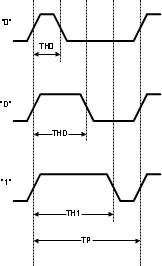 Figure 1. Single-Wire Interface (SWIF) Timing Diagram
6.7 Typical Characteristics
At TA = TJ = 25°C, Loop Voltage = 20V to 36V, unless otherwise specified.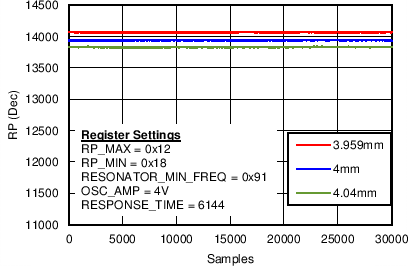
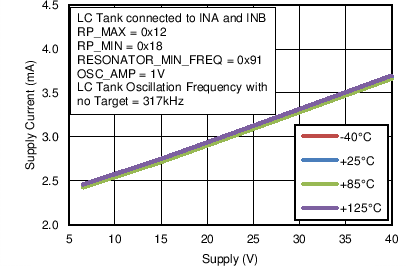
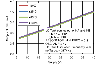
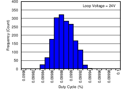 Figure 8. 0.1% Duty Cycle Distribution, PNP Mode
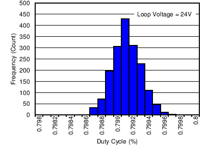 Figure 10. 0.8% Duty Cycle Distribution, PNP Mode
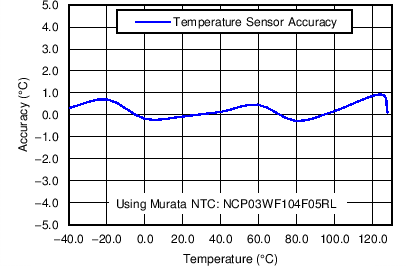
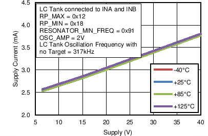
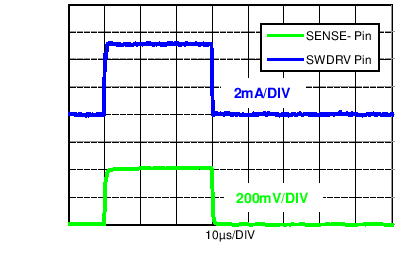
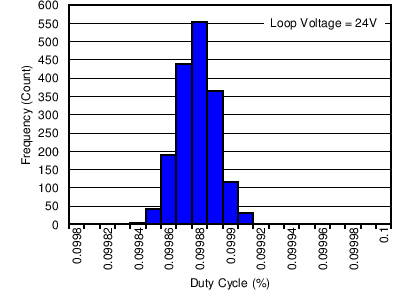 Figure 9. 0.1% Duty Cycle Distribution, NPN Mode
 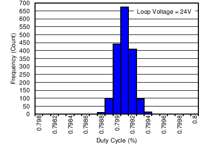 Figure 11. 0.8% Duty Cycle Distribution, NPN Mode
 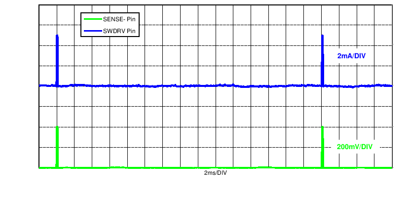 Figure 12. SWDRV and SENSE- Waveforms During Short Condition, SHORTCKT_DUTY_CYCLE = 0.1%
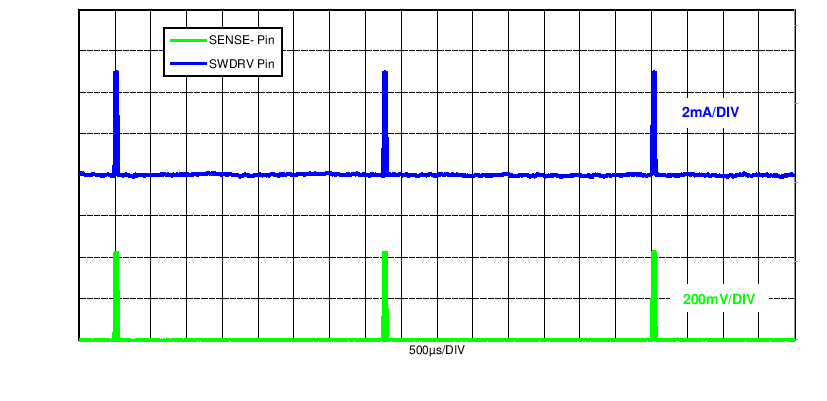 Figure 13. SWDRV and SENSE- Waveforms During Short Condition, SHORTCKT_DUTY_CYCLE = 0.8%