SNOSCX0A June 2013 – December 2014 LMP92064
PRODUCTION DATA.
- 1 Features
- 2 Applications
- 3 Description
- 4 Revision History
- 5 Pin Configuration and Functions
- 6 Specifications
- 7 Detailed Description
- 8 Application and Implementation
- 9 Power Supply Recommendations
- 10Layout
- 11Device and Documentation Support
- 12Mechanical, Packaging, and Orderable Information
Package Options
Mechanical Data (Package|Pins)
- NHR|16
Thermal pad, mechanical data (Package|Pins)
Orderable Information
8 Application and Implementation
NOTE
Information in the following applications sections is not part of the TI component specification, and TI does not warrant its accuracy or completeness. TI’s customers are responsible for determining suitability of components for their purposes. Customers should validate and test their design implementation to confirm system functionality.
8.1 Application Information
The LMP92064 is a precision low-side digital current sensor and voltage monitor with a digital SPI interface. The device is typically used to measure a load current by means of a current sense resistor connected in series with a load. Use the following design procedure to select the main components of a simple current and voltage monitoring application using the LMP92064.
8.2 Typical Application
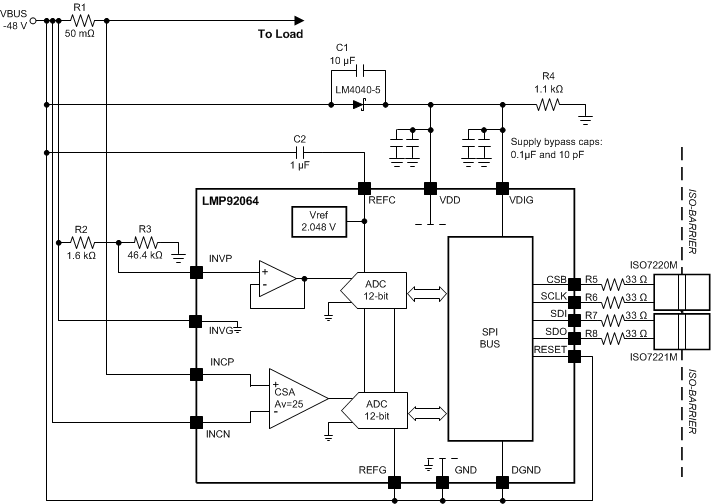
In this example, the LMP92064 is used to sense the load current flowing through the sense resistor, R1. Additionally, the voltage across R3 can be sensed to calculate the bus voltage.
The load that will be monitored is operating from a –48-V bus. Because the GND pin of the LMP92064 is connected to the –48-V bus, –48 V becomes the ground reference for the device.
 Figure 23. Typical Application Diagram
8.2.1 Design Requirements
For this design example, use the parameters listed in Table 4 as the application parameters.
Table 4. Design Parameters
| DESIGN PARAMETER | EXAMPLE VALUE |
|---|---|
| Bus Voltage | -48 V |
| Bus Voltage Variation | ±2% |
| Supply Voltage | 5 V |
| SPI Clock | 12 MHz |
| Maximum Load Current | 1 A |
| Resolution | 1 mA |
8.2.2 Detailed Design Procedure
8.2.2.1 Digital Isolators
The ISO7220M and ISO7221M isolators are used for this example. Please refer to the ISO722x documentation for device specific information. These devices support data rates of up to 150 Mbps and provide a low propagation delay necessary for bi-directional SPI communication at 12 MHz.
8.2.2.2 Supply Voltage for the LMP92064
A 5-V supply is required for the LMP92064. The LM4040-5 reference is used to generate the required voltage from the load’s –48-V supply. The LM4040-N is a precision micropower shunt voltage reference and is available in several fixed breakdown voltage options. The LM4040-5 provides the required 5-V breakdown voltage.
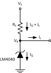
In a conventional shunt regulator application (Figure 24), the LM4040-5 requires a current limiting resistor connected between the positive supply voltage and the LM4040-5.
 Figure 24. Shunt Regulator
The value of the resistor is determined by the positive supply voltage (VS), the load current (IL), the reference operating current (IQ), and the LM4040-5’s reverse breakdown voltage (VR).

8.2.2.3 Series Resistor for the Shunt Regulator
The selection of RS should satisfy two main conditions:
- RS should be small enough to supply at least the minimum acceptable IQ to the LM4040-5 even when the supply voltage is at its minimum and the load current is at its maximum value.
- RS should be large enough so that the current flowing through the LM4040-5 is less than 15 mA when the supply voltage is at its maximum and the load current is at its minimum.
The minimum operating current of the LM4040AIM3-5/NOPB is 80 μA and its maximum operating current is 15 mA.
The typical supply current of the LMP92064 is 13 mA. The measured average current of the circuit, including the isolators, is 38 mA.
 Figure 25. Shunt Regulator Voltages
From Figure 25, VS = 0 V and VR = –43 V. RS can be calculated as follows:

Choosing a smaller resistor, like a 1.1-kΩ resistor, will result in about 39.1 mA to flowing through RS, providing a margin of 1 mA above the required 38.08 mA.
A variation in the bus voltage (VBUS) of ±2% would result in less than ±0.87 mA of current variation. Given the additional current margin obtained by the 1.1-kΩ resistor, the shunt regulator would still have more than the required 80 μA of operating current.
The power rating of the series resistor should be selected according to the expected power to be dissipated. In normal operation, the resistor would dissipate 43 V x 39 mA = 1.677 W.
Excess current not used by the LMP92064 and isolators circuits will be burned by in the LM4040-5, and this current should never exceed 15 mA.
8.2.2.4 Voltage Channel Input Resistor Divider
The input buffer amplifier of the LMP92064's voltage channel can tolerate high source impedances, which enables scaling the bus voltage with the use of an external resistor divider. The accuracy of the voltage measurements depends on the accuracy of the components used for the resistor divider as well as the impedance of the divider.
In this example, the voltage channel can sense the voltage across R2 (see Figure 23). The main voltage should be scaled to a range below 2.048V by the resistive divider. If the resistive divider is always connected to the bus voltage, the series resistance of R2 + R3 should be adjusted (while keeping their ratio constant) to limit the current across the resistors within a permissible range for the application.
For simplicity, R2 is set to 1.6kΩ and R3 is set to 46.4 kΩ. The bus voltage of 48 V results in 1.6 V across R2 and the current flowing through R2 and R3 is 1 mA.
8.2.2.5 Sense Resistor Selection
The accuracy of the current measurement depends heavily on the accuracy of the current sense resistor. Its value depends on the application and it is a compromise between signal accuracy, maximum permissible voltage loss and power dissipation in the current sense resistor. High resistance values provide better accuracy at lower currents by minimizing the effects of offset, while low resistance values of minimize voltage loss in the load supply section, but at the expense of low-end accuracy.
In this example, the maximum sense voltage at the input of the current sense channel of the LMP92064 is 75 mV. Given the maximum load current requirement of 1 A, the sense resistor should be selected to be smaller than 75 mΩ.
The resolution at the input of the current sense channel of the device is 20 μV / code. To observe a change in the output code for a 1 mA change in sense current, the sense resistor should be larger than 20 mΩ.
8.2.3 Application Curves
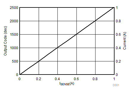
The data in the following curves was collected using a 50 mΩ sense resistor, which results in a conversion factor of 2.5 codes/mA. The sense current for the first curve was increased in steps of 100 mA up to 1 A. The sense current for the second curve was increased in steps of 1 mA up to 10 mA. The data was acquired asynchronously at a rate of 2000 samples per second, and each data point is the resulting average of 260 samples.
 Figure 26. Output Codes in 1-A Range
 Figure 27. Output Codes in 10-mA Range