SNVSBR8D March 2020 – June 2022 LMQ61460
PRODUCTION DATA
- 1 Features
- 2 Applications
- 3 Description
- 4 Revision History
- 5 Device Comparison Table
- 6 Pin Configuration and Functions
- 7 Specifications
-
8 Detailed Description
- 8.1 Overview
- 8.2 Functional Block Diagram
- 8.3
Feature Description
- 8.3.1 EN/SYNC Uses for Enable and VIN UVLO
- 8.3.2 EN/SYNC Pin Uses for Synchronization
- 8.3.3 Adjustable Switching Frequency
- 8.3.4 Clock Locking
- 8.3.5 PGOOD Output Operation
- 8.3.6 Internal LDO, VCC UVLO, and BIAS Input
- 8.3.7 Bootstrap Voltage and VCBOOT-UVLO (CBOOT Pin)
- 8.3.8 Adjustable SW Node Slew Rate
- 8.3.9 Spread Spectrum
- 8.3.10 Soft Start and Recovery From Dropout
- 8.3.11 Output Voltage Setting
- 8.3.12 Overcurrent and Short Circuit Protection
- 8.3.13 Thermal Shutdown
- 8.3.14 Input Supply Current
- 8.4 Device Functional Modes
- 9 Application and Implementation
- 10Power Supply Recommendations
- 11Layout
- 12Device and Documentation Support
- 13Mechanical, Packaging, and Orderable Information
Package Options
Mechanical Data (Package|Pins)
- RJR|14
Thermal pad, mechanical data (Package|Pins)
Orderable Information
8.3.10 Soft Start and Recovery From Dropout
The device uses a reference-based soft start that prevents output voltage overshoots and large inrush currents during start-up. Soft start is triggered by any of the following conditions:
- Power is applied to the VIN pin of the IC, releasing UVLO.
- EN is used to turn on the device.
- Recovery from a hiccup waiting period
- Recovery from shutdown due to overtemperature protection
Once soft start is triggered, the IC takes the following actions:
- The reference used by the IC to regulate output voltage is slowly ramped. The net result is that output voltage takes tSS to reach 90% of its desired value.
- Operating mode is set to auto, activating diode emulation, which allows start-up without pulling output low if there is a voltage already present on output.
Together, these actions provide start-up with limited inrush currents and also allow the use of larger output capacitors and higher loading conditions that cause current to border on current limit during start-up without triggering hiccup. See Figure 8-8.

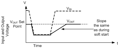
Any time the output voltage falls more than a few percent, the output voltage ramps up slowly. This condition is called recovery from dropout and differs from soft start in three important ways:
- The reference voltage is set to approximately 1% above what is needed to achieve the existing output voltage.
- Hiccup is allowed if output voltage is less than 0.4 times its set point. Note that during dropout regulation itself, hiccup is inhibited.
- FPWM mode is allowed during recovery from dropout. If the output voltage were to suddenly be pulled up by an external supply, the device can pull down on the output.
Despite being called recovery from dropout, this feature is active whenever output voltage drops to a few percent lower than the set point, which primarily occurs under the following conditions:
- Dropout: When there is insufficient input voltage for the desired output voltage to be generated
- Overcurrent: When there is an overcurrent event that is not severe enough to trigger hiccup

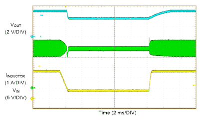
 Figure 8-10 Recovery From Dropout (VOUT = 5 V, IOUT = 4 A, VIN = 13.5 V to 4 V to 13.5 V)