SNVS731B September   2011  – June 2019 LMR12010

PRODUCTION DATA.  

  1. Features
  2. Applications
  3. Description
    1.     Device Images
      1.      Typical Application
  4. Revision History
  5. Pin Configuration and Functions
    1.     Pin Descriptions
  6. Specifications
    1. 6.1 Absolute Maximum Ratings
    2. 6.2 Recommended Operating Ratings
    3. 6.3 Electrical Characteristics
    4. 6.4 Typical Characteristics
  7. Detailed Description
    1. 7.1 Overview
    2. 7.2 Functional Block Diagram
    3. 7.3 Feature Description
      1. 7.3.1 Boost Function
      2. 7.3.2 Enable Pin / Shutdown Mode
      3. 7.3.3 Soft Start
      4. 7.3.4 Output Overvoltage Protection
      5. 7.3.5 Undervoltage Lockout
      6. 7.3.6 Current Limit
      7. 7.3.7 Thermal Shutdown
  8. Application and Implementation
    1. 8.1 Application Information
    2. 8.2 Typical Application
      1.      Typical Application
      2. 8.2.1 Detailed Design Procedure
        1. 8.2.1.1 Custom Design With WEBENCH® Tools
        2. 8.2.1.2 Inductor Selection
        3. 8.2.1.3 Input Capacitor
        4. 8.2.1.4 Output Capacitor
        5. 8.2.1.5 Catch Diode
        6. 8.2.1.6 Boost Diode
        7. 8.2.1.7 Boost Capacitor
        8. 8.2.1.8 Output Voltage
        9. 8.2.1.9 Calculating Efficiency, and Junction Temperature
      3. 8.2.2 Application Curves
  9. Layout
    1. 9.1 Layout Considerations
    2. 9.2 Calculating The LMR12010 Junction Temperature
  10. 10Device and Documentation Support
    1. 10.1 Device Support
      1. 10.1.1 Third-Party Products Disclaimer
      2. 10.1.2 Development Support
        1. 10.1.2.1 Custom Design With WEBENCH® Tools
    2. 10.2 Receiving Notification of Documentation Updates
    3. 10.3 Community Resources
    4. 10.4 Trademarks
    5. 10.5 Electrostatic Discharge Caution
    6. 10.6 Glossary
  11. 11Mechanical, Packaging, and Orderable Information

Package Options

Refer to the PDF data sheet for device specific package drawings

Mechanical Data (Package|Pins)
  • DDC|6
Thermal pad, mechanical data (Package|Pins)
Orderable Information

Application Curves

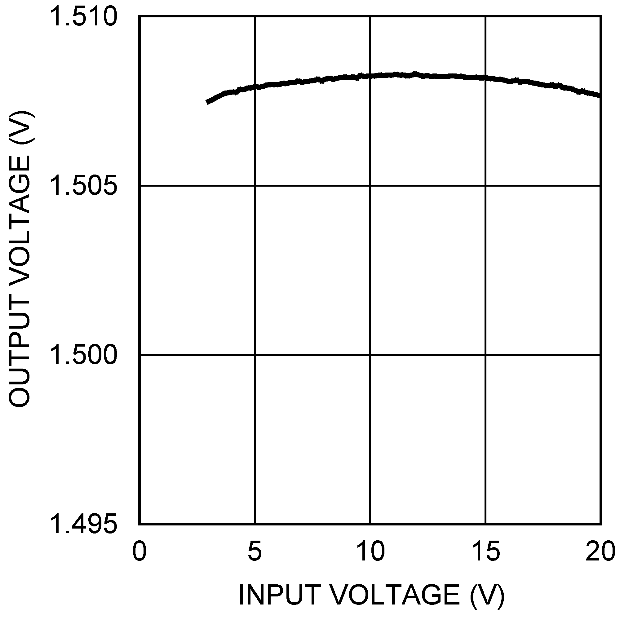
LMR12010 30166556.png
VOUT = 1.5 V IOUT = 500 mA
Figure 21. Line Regulation - "X"
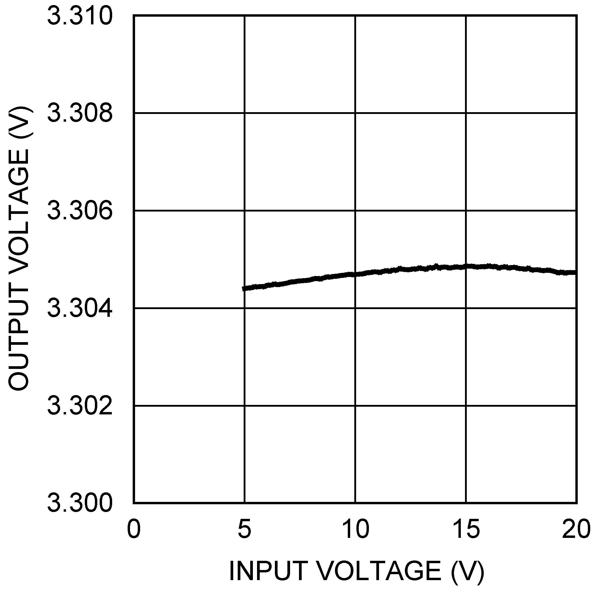
LMR12010 30166555.png
VOUT = 3.3 V IOUT = 500 mA
Figure 23. Line Regulation - "X"
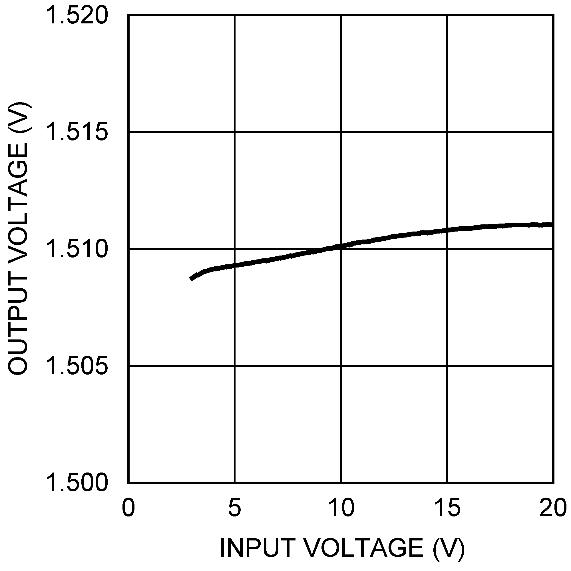
LMR12010 30166554.png
VOUT = 1.5 V IOUT = 500 mA
Figure 22. Line Regulation - "Y"
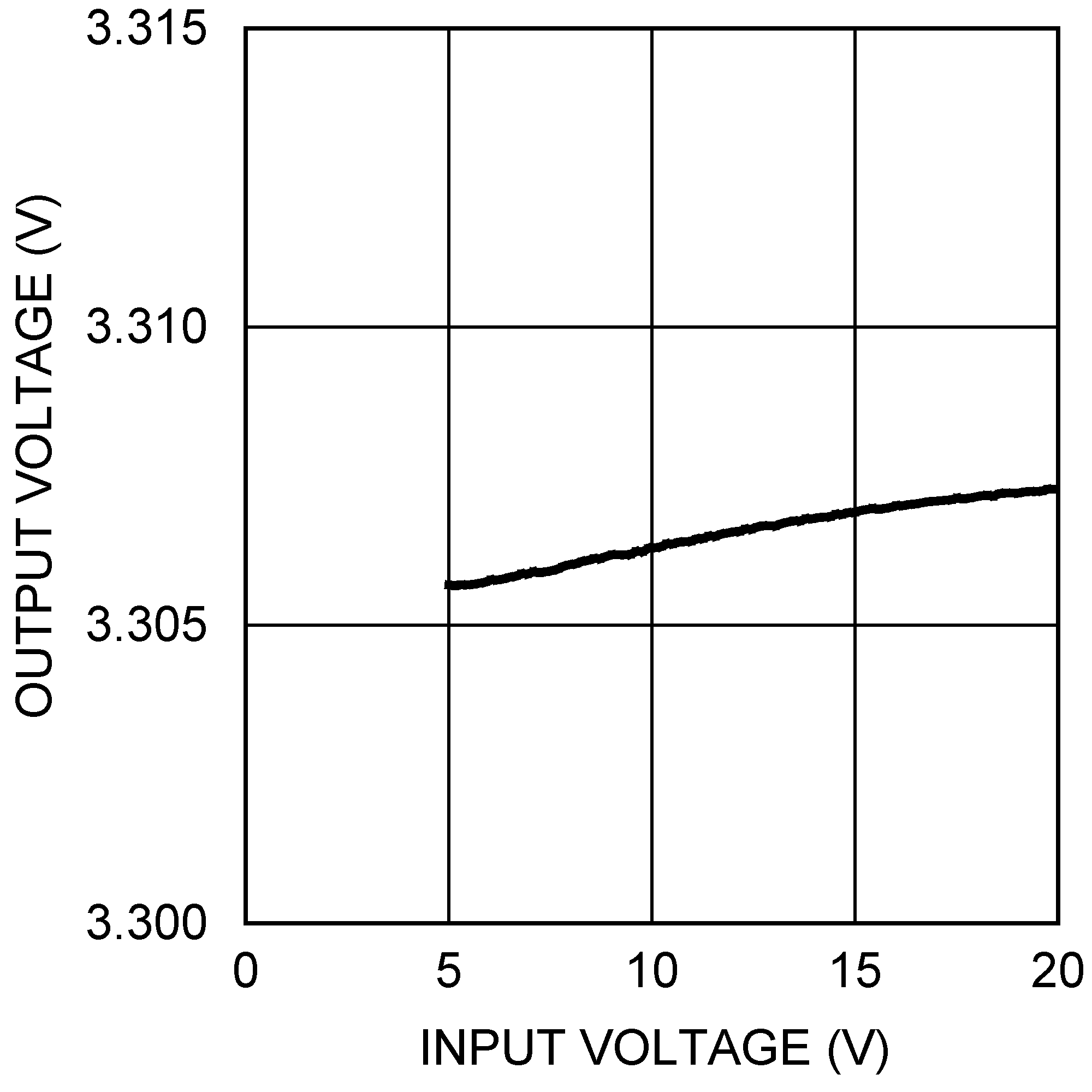
LMR12010 30166553.png
VOUT = 3.3 V IOUT = 500 mA
Figure 24. Line Regulation - "Y"