SNVSAG3B November   2015  – December 2024 LMR14030-Q1

PRODUCTION DATA  

  1.   1
  2. Features
  3. Applications
  4. Description
  5. Pin Configuration and Functions
  6. Specifications
    1. 5.1 Absolute Maximum Ratings
    2. 5.2 ESD Ratings
    3. 5.3 Recommended Operating Conditions
    4. 5.4 Thermal Information
    5. 5.5 Electrical Characteristics
    6. 5.6 Switching Characteristics
    7. 5.7 Typical Characteristics
  7. Detailed Description
    1. 6.1 Overview
    2. 6.2 Functional Block Diagram
    3. 6.3 Feature Description
      1. 6.3.1  Fixed Frequency Peak Current Mode Control
      2. 6.3.2  Slope Compensation
      3. 6.3.3  Sleep-mode
      4. 6.3.4  Low Dropout Operation and Bootstrap Voltage (BOOT)
      5. 6.3.5  Adjustable Output Voltage
      6. 6.3.6  Enable and Adjustable Undervoltage Lockout
      7. 6.3.7  External Soft-start
      8. 6.3.8  Switching Frequency and Synchronization (RT/SYNC)
      9. 6.3.9  Power Good (PGOOD)
      10. 6.3.10 Over Current and Short Circuit Protection
      11. 6.3.11 Overvoltage Protection
      12. 6.3.12 Thermal Shutdown
    4. 6.4 Device Functional Modes
      1. 6.4.1 Shutdown Mode
      2. 6.4.2 Active Mode
      3. 6.4.3 CCM Mode
      4. 6.4.4 Light Load Operation
  8. Application and Implementation
    1. 7.1 Application Information
    2. 7.2 Typical Application
      1. 7.2.1 Design Requirements
      2. 7.2.2 Detailed Design Procedure
        1. 7.2.2.1 Output Voltage Set-Point
        2. 7.2.2.2 Switching Frequency
        3. 7.2.2.3 Output Inductor Selection
        4. 7.2.2.4 Output Capacitor Selection
        5. 7.2.2.5 Schottky Diode Selection
        6. 7.2.2.6 Input Capacitor Selection
        7. 7.2.2.7 Bootstrap Capacitor Selection
        8. 7.2.2.8 Soft-start Capacitor Selection
      3. 7.2.3 Application Curves
    3. 7.3 Power Supply Recommendations
    4. 7.4 Layout
      1. 7.4.1 Layout Guidelines
      2. 7.4.2 Layout Example
  9. Device and Documentation Support
    1. 8.1 Device Support
      1. 8.1.1 Third-Party Products Disclaimer
    2. 8.2 Documentation Support
      1. 8.2.1 Related Documentation
      2. 8.2.2 Related Products
    3. 8.3 Receiving Notification of Documentation Updates
    4. 8.4 Support Resources
    5. 8.5 Trademarks
    6. 8.6 Electrostatic Discharge Caution
    7. 8.7 Glossary
  10. Revision History
  11. 10Mechanical, Packaging, and Orderable Information

Package Options

Mechanical Data (Package|Pins)
Thermal pad, mechanical data (Package|Pins)
Orderable Information

Application Curves

Unless otherwise specified the following conditions apply: VIN = 12 V, fSW = 500 kHz, L = 5.6 µH, COUT = 47 µF × 2, TA = 25 °C.
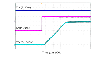
LMR14030-Q1 Start-up By EN
VIN = 12 VVOUT = 5 VIOUT = 2 A
Figure 7-2 Start-up By EN
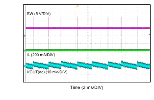
LMR14030-Q1 Sleep-mode
VIN = 12 VVOUT = 5 VIOUT = 0 A
Figure 7-4 Sleep-mode
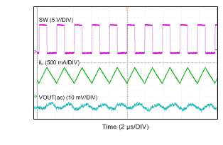
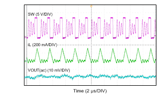
LMR14030-Q1 CCM Mode
VIN = 12 VVOUT = 5 VIOUT = 1.5 A
Figure 7-6 CCM Mode
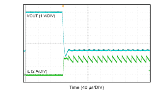
LMR14030-Q1 Output Short
VIN = 12 VVOUT = 5 V
Figure 7-8 Output Short
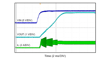
LMR14030-Q1 Start-up By VIN
VIN = 12 VVOUT = 5 VIOUT = 2 A
Figure 7-3 Start-up By VIN
LMR14030-Q1 DCM Mode
VIN = 12 VVOUT = 5 VIOUT = 100 mA
Figure 7-5 DCM Mode
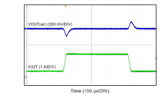
LMR14030-Q1 Load Transient
IOUT: 20% → 80% of 3.5 ASlew rate = 100 mA/μs
Figure 7-7 Load Transient
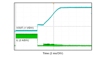
LMR14030-Q1 Output Short Recovery
VIN = 12 VVOUT = 5 V
Figure 7-9 Output Short Recovery