SNVSAC1 June 2015 LMR16006Y-Q1
PRODUCTION DATA.
- 1 Features
- 2 Applications
- 3 Description
- 4 Simplified Schematic
- 5 Revision History
- 6 Pin Configuration and Functions
- 7 Specifications
- 8 Detailed Description
- 9 Application and Implementation
- 10Power Supply Recommendations
- 11Layout
- 12Device and Documentation Support
- 13Mechanical, Packaging, and Orderable Information
Package Options
Mechanical Data (Package|Pins)
- DDC|6
Thermal pad, mechanical data (Package|Pins)
Orderable Information
11 Layout
11.1 Layout Guidelines
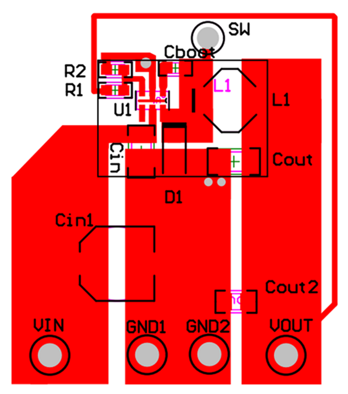
Layout is a critical portion of good power supply design. The following guidelines will help users design a PCB with the best power conversion performance, thermal performance, and minimized generation of unwanted EMI.
- The feedback network, resistors R1 and R2, should be kept close to the FB pin, and away from the inductor to minimize coupling noise into the feedback pin.
- The input bypass capacitor Cin must be placed close to the VIN pin. This will reduce copper trace resistance which effects input voltage ripple of the IC.
- The inductor L1 should be placed close to the SW pin to reduce magnetic and electrostatic noise.
- The output capacitor, Cout should be placed close to the junction of L1 and the diode D1. The L1, D1, and Cout trace should be as short as possible to reduce conducted and radiated noise and increase overall efficiency.
- The ground connection for the diode, Cin, and Cout should be as small as possible and tied to the system ground plane in only one spot (preferably at the Cout ground point) to minimize conducted noise in the system ground plane.
- For more detail on switching power supply layout considerations see AN-1149 Layout Guidelines for Switching Power Supplies SNVA021
11.2 Layout Example
 Figure 15. Layout