SNVSAR4A December 2016 – April 2017 LMR23610-Q1
PRODUCTION DATA.
- 1 Features
- 2 Applications
- 3 Description
- 4 Revision History
- 5 Pin Configuration and Functions
- 6 Specifications
-
7 Detailed Description
- 7.1 Overview
- 7.2 Functional Block Diagram
- 7.3
Feature Description
- 7.3.1 Fixed Frequency Peak Current Mode Control
- 7.3.2 Adjustable Output Voltage
- 7.3.3 Enable/Sync
- 7.3.4 VCC, UVLO
- 7.3.5 Minimum ON-time, Minimum OFF-time and Frequency Foldback at Drop-out Conditions
- 7.3.6 Internal Compensation and CFF
- 7.3.7 Bootstrap Voltage (BOOT)
- 7.3.8 Over Current and Short Circuit Protection
- 7.3.9 Thermal Shutdown
- 7.4 Device Functional Modes
-
8 Application and Implementation
- 8.1 Application Information
- 8.2
Typical Applications
- 8.2.1 Design Requirements
- 8.2.2
Detailed Design Procedure
- 8.2.2.1 Custom Design With WEBENCH® Tools
- 8.2.2.2 Output Voltage Set-Point
- 8.2.2.3 Switching Frequency
- 8.2.2.4 Inductor Selection
- 8.2.2.5 Output Capacitor Selection
- 8.2.2.6 Feed-Forward Capacitor
- 8.2.2.7 Input Capacitor Selection
- 8.2.2.8 Bootstrap Capacitor Selection
- 8.2.2.9 VCC Capacitor Selection
- 8.2.2.10 Under Voltage Lockout Set-Point
- 8.2.3 Application Curves
- 9 Power Supply Recommendations
- 10Layout
- 11Device and Documentation Support
- 12Mechanical, Packaging, and Orderable Information
Package Options
Refer to the PDF data sheet for device specific package drawings
Mechanical Data (Package|Pins)
- DDA|8
Thermal pad, mechanical data (Package|Pins)
- DDA|8
Orderable Information
7 Detailed Description
7.1 Overview
The LMR23610-Q1 SIMPLE SWITCHER® regulator is an easy to use synchronous step-down DC-DC converter operating from 4 V to 36 V supply voltage. It is capable of delivering up to 1 A DC load current with good thermal performance in a small solution size. An extended family is available in multiple current options from 1 A to 3 A in pin-to-pin compatible packages.
The LMR23610-Q1 employs fixed frequency peak current mode control. The device enters PFM mode at light load to achieve high efficiency. The device is internally compensated, which reduces design time, and requires few external components. The LMR23610-Q1 is capable of synchronization to an external clock within the range of 200 kHz to 2.2 MHz.
Additional features such as precision enable and internal soft-start provide a flexible and easy to use solution for a wide range of applications. Protection features include thermal shutdown, VIN and VCC under-voltage lockout, cycle-by-cycle current limit, and hiccup mode short-circuit protection.
The family requires very few external components and has a pin-out designed for simple, optimum PCB layout.
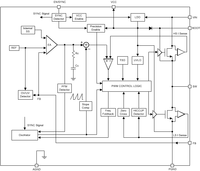
7.2 Functional Block Diagram
7.3 Feature Description
7.3.1 Fixed Frequency Peak Current Mode Control
The following operating description of the LMR23610-Q1 will refer to the Functional Block Diagram and to the waveforms in Figure 13. LMR23610-Q1 is a step-down synchronous buck regulator with integrated high-side (HS) and low-side (LS) switches (synchronous rectifier). The LMR23610-Q1 supplies a regulated output voltage by turning on the HS and LS NMOS switches with controlled duty cycle. During high-side switch ON time, the SW pin voltage swings up to approximately VIN, and the inductor current iL increase with linear slope (VIN – VOUT) / L. When the HS switch is turned off by the control logic, the LS switch is turned on after an anti-shoot-through dead time. Inductor current discharges through the LS switch with a slope of –VOUT / L. The control parameter of a buck converter is defined as Duty Cycle D = tON / TSW, where tON is the high-side switch ON time and TSW is the switching period. The regulator control loop maintains a constant output voltage by adjusting the duty cycle D. In an ideal buck converter, where losses are ignored, D is proportional to the output voltage and inversely proportional to the input voltage: D = VOUT / VIN.
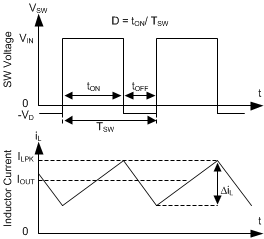 Figure 13. SW Node and Inductor Current Waveforms in
 Continuous Conduction Mode (CCM)
The LMR23610-Q1 employs fixed frequency peak current mode control. A voltage feedback loop is used to get accurate DC voltage regulation by adjusting the peak current command based on voltage offset. The peak inductor current is sensed from the high-side switch and compared to the peak current threshold to control the ON time of the high-side switch. The voltage feedback loop is internally compensated, which allows for fewer external components, makes it easy to design, and provides stable operation with almost any combination of output capacitors. The regulator operates with fixed switching frequency at normal load condition. At light load condition, the LMR23610-Q1 will operate in PFM mode to maintain high efficiency.
7.3.2 Adjustable Output Voltage
A precision 1.0 V reference voltage is used to maintain a tightly regulated output voltage over the entire operating temperature range. The output voltage is set by a resistor divider from output voltage to the FB pin. It is recommended to use 1% tolerance resistors with a low temperature coefficient for the FB divider. Select the low-side resistor RFBB for the desired divider current and use Equation 1 to calculate high-side RFBT. RFBT in the range from 10 kΩ to 100 kΩ is recommended for most applications. A lower RFBT value can be used if static loading is desired to reduce VOUT offset in PFM operation. Lower RFBT will reduce efficiency at very light load. Less static current goes through a larger RFBT and might be more desirable when light load efficiency is critical. But RFBT larger than 1 MΩ is not recommended because it makes the feedback path more susceptible to noise. Larger RFBT value requires more carefully designed feedback path on the PCB. The tolerance and temperature variation of the resistor dividers affect the output voltage regulation.
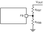 Figure 14. Output Voltage Setting

7.3.3 Enable/Sync
The voltage on the EN pin controls the ON or OFF operation of LMR23610-Q1. A voltage less than 1 V (typ) will shut-down the device while a voltage higher than 1.6 V (typ) is required to start the regulator. The EN pin is an input and can not be left open or floating. The simplest way to enable the operation of the LMR23610-Q1 is to connect the EN to VIN. This allows self-start-up of the LMR23610-Q1 when VIN is within the operation range.
Many applications will benefit from the employment of an enable divider RENT and RENB (Figure 15) to establish a precision system UVLO level for the converter. System UVLO can be used for supplies operating from utility power as well as battery power. It can be used for sequencing, ensuring reliable operation, or supply protection, such as a battery discharge level. An external logic signal can also be used to drive EN input for system sequencing and protection.
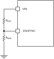 Figure 15. System UVLO by Enable Divider
The EN pin also can be used to synchronize the internal oscillator to an external clock. The internal oscillator can be synchronized by AC coupling a positive edge into the EN pin. The AC coupled peak-to-peak voltage at the EN pin must exceed the SYNC amplitude threshold of 2.8 V (typ) to trip the internal synchronization pulse detector, and the minimum SYNC clock ON and OFF time must be longer than 100ns (typ). A 3.3 V or a higher amplitude pulse signal coupled through a 1 nF capacitor CSYNC is a good starting point. Keeping RENT // RENB (RENT parallel with RENB) in the 100 kΩ range is a good choice. RENT is required for this synchronization circuit, but RENB can be left unmounted if system UVLO is not needed. LMR23610-Q1 switching action can be synchronized to an external clock from 200 kHz to 2.2 MHz. Figure 17 and Figure 18 show the device synchronized to an external system clock.
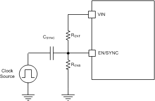 Figure 16. Synchronize to external clock
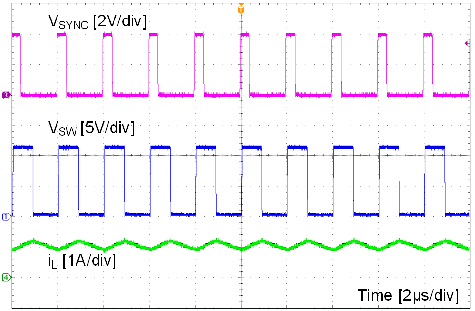 Figure 17. Synchronizing in PWM Mode
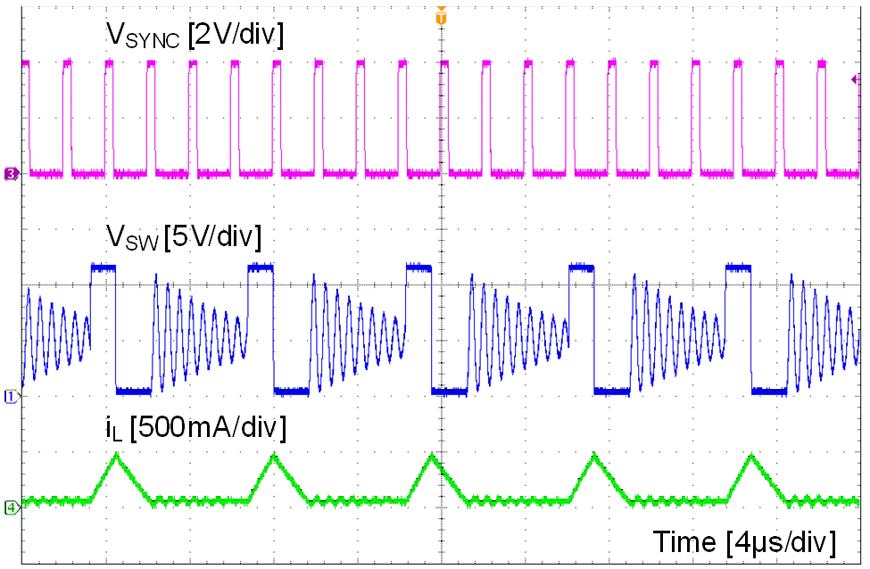 Figure 18. Synchronizing in PFM Mode
7.3.4 VCC, UVLO
The LMR23610-Q1 integrates an internal LDO to generate VCC for control circuitry and MOSFET drivers. The nominal voltage for VCC is 4.1 V. The VCC pin is the output of an LDO and must be properly bypassed. A high quality ceramic capacitor with a value of 2.2 µF to 10 µF, 16 V or higher rated voltage should be placed as close as possible to VCC and grounded to the exposed PAD and ground pins. The VCC output pin should not be loaded, or shorted to ground during operation. Shorting VCC to ground during operation may cause damage to the LMR23610-Q1.
VCC under voltage lockout (UVLO) prevents the LMR23610-Q1 from operating until the VCC voltage exceeds 3.2 V (typ). The VCC UVLO threshold has 400 mV (typ) of hysteresis to prevent undesired shutdown due to temporary VIN drops.
7.3.5 Minimum ON-time, Minimum OFF-time and Frequency Foldback at Drop-out Conditions
Minimum ON-time, TON_MIN, is the smallest duration of time that the HS switch can be on. TON_MIN is typically 60 ns in the LMR23610-Q1. Minimum OFF-time, TOFF_MIN, is the smallest duration that the HS switch can be off. TOFF_MIN is typically 100 ns in the LMR23610-Q1. In CCM operation, TON_MIN and TOFF_MIN limit the voltage conversion range given a selected switching frequency.
The minimum duty cycle allowed is:
And the maximum duty cycle allowed is:
Given fixed TON_MIN and TOFF_MIN, the higher the switching frequency the narrower the range of the allowed duty cycle. In the LMR23610-Q1, a frequency foldback scheme is employed to extend the maximum duty cycle when TOFF_MIN is reached. The switching frequency will decrease once longer duty cycle is needed under low VIN conditions. Wide range of frequency foldback allows the LMR23610-Q1 output voltage stay in regulation with a much lower supply voltage VIN. This leads to a lower effective drop-out voltage.
Given an output voltage, the choice of the switching frequency affects the allowed input voltage range, solution size and efficiency. The maximum operation supply voltage can be found by:

At lower supply voltage, the switching frequency will decrease once TOFF_MIN is tripped. The minimum VIN without frequency foldback can be approximated by:

Taking considerations of power losses in the system with heavy load operation, VIN_MAX is higher than the result calculated in Equation 4. With frequency foldback, VIN_MIN is lowered by decreased fSW.
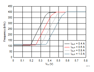 Figure 19. Frequency Foldback at Dropout (VOUT = 5 V, fSW = 400 kHz)
7.3.6 Internal Compensation and CFF
The LMR23610-Q1 is internally compensated as shown in Functional Block Diagram. The internal compensation is designed such that the loop response is stable over the entire operating frequency and output voltage range. Depending on the output voltage, the compensation loop phase margin can be low with all ceramic capacitors. An external feed-forward capacitor CFF is recommended to be placed in parallel with the top resistor divider RFBT for optimum transient performance.
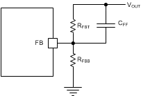 Figure 20. Feedforward Capacitor for Loop Compensation
The feed-forward capacitor CFF in parallel with RFBT places an additional zero before the cross over frequency of the control loop to boost phase margin. The zero frequency can be found by

An additional pole is also introduced with CFF at the frequency of

The zero fZ_CFF adds phase boost at the crossover frequency and improves transient response. The pole fP-CFF helps maintaining proper gain margin at frequency beyond the crossover. Table 1 lists the combination of COUT, CFF and RFBT for typical applications, designs with similar COUT but RFBT other than recommended value, please adjust CFF such that (CFF × RFBT) is unchanged and adjust RFBB such that (RFBT / RFBB) is unchanged.
Designs with different combinations of output capacitors need different CFF. Different types of capacitors have different Equivalent Series Resistance (ESR). Ceramic capacitors have the smallest ESR and need the most CFF. Electrolytic capacitors have much larger ESR and the ESR zero frequency

would be low enough to boost the phase up around the crossover frequency. Designs using mostly electrolytic capacitors at the output may not need any CFF.
The CFF creates a time constant with RFBT that couples in the attenuate output voltage ripple to the FB node. If the CFF value is too large, it can couple too much ripple to the FB and affect VOUT regulation. Therefore, CFF should be calculated based on output capacitors used in the system. At cold temperatures, the value of CFF might change based on the tolerance of the chosen component. This may reduce its impedance and ease noise coupling on the FB node. To avoid this, more capacitance can be added to the output or the value of CFF can be reduced.
7.3.7 Bootstrap Voltage (BOOT)
The LMR23610-Q1 provides an integrated bootstrap voltage regulator. A small capacitor between the BOOT and SW pins provides the gate drive voltage for the high-side MOSFET. The BOOT capacitor is refreshed when the high-side MOSFET is off and the low-side switch conducts. The recommended value of the BOOT capacitor is 0.1 μF. A ceramic capacitor with an X7R or X5R grade dielectric with a voltage rating of 16V or higher is recommended for stable performance over temperature and voltage.
7.3.8 Over Current and Short Circuit Protection
The LMR23610-Q1 is protected from over-current conditions by cycle-by-cycle current limit on both the peak and valley of the inductor current. Hiccup mode will be activated if a fault condition persists to prevent over-heating.
High-side MOSFET over-current protection is implemented by the nature of the Peak Current Mode control. The HS switch current is sensed when the HS is turned on after a set blanking time. The HS switch current is compared to the output of the Error Amplifier (EA) minus slope compensation every switching cycle. Please refer to Functional Block Diagram for more details. The peak current of HS switch is limited by a clamped maximum peak current threshold IHS_LIMIT which is constant. So the peak current limit of the high-side switch is not affected by the slope compensation and remains constant over the full duty cycle range.
The current going through LS MOSFET is also sensed and monitored. When the LS switch turns on, the inductor current begins to ramp down. The LS switch will not be turned OFF at the end of a switching cycle if its current is above the LS current limit ILS_LIMIT. The LS switch will be kept ON so that inductor current keeps ramping down, until the inductor current ramps below the LS current limit ILS_LIMIT. Then the LS switch will be turned OFF and the HS switch will be turned on after a dead time. This is somewhat different than the more typical peak current limit, and results in Equation 9 for the maximum load current.

If the current of the LS switch is higher than the LS current limit for 64 consecutive cycles, hiccup current protection mode will be activated. In hiccup mode, the regulator will be shut down and kept off for 5 ms typically before the LMR23610-Q1 tries to start again. If over-current or short-circuit fault condition still exist, hiccup will repeat until the fault condition is removed. Hiccup mode reduces power dissipation under severe over-current conditions, prevents over-heating and potential damage to the device.
7.3.9 Thermal Shutdown
The LMR23610-Q1 provides an internal thermal shutdown to protect the device when the junction temperature exceeds 170 °C (typ). The device is turned off when thermal shutdown activates. Once the die temperature falls below 155 °C (typ), the device reinitiates the power up sequence controlled by the internal soft-start circuitry.
7.4 Device Functional Modes
7.4.1 Shutdown Mode
The EN pin provides electrical ON and OFF control for the LMR23610-Q1. When VEN is below 1 V (typ), the device is in shutdown mode. The LMR23610-Q1 also employs VIN and VCC under voltage lock out protection. If VIN or VCC voltage is below their respective UVLO level, the regulator will be turned off.
7.4.2 Active Mode
The LMR23610-Q1 is in Active Mode when VEN is above the precision enable threshold, VIN and VCC are above their respective UVLO level. The simplest way to enable the LMR23610-Q1 is to connect the EN pin to VIN pin. This allows self startup when the input voltage is in the operating range: 4 V to 36 V. Please refer to VCC, UVLO and Enable/Sync for details on setting these operating levels.
In Active Mode, depending on the load current, the LMR23610-Q1 will be in one of three modes:
- Continuous conduction mode (CCM) with fixed switching frequency when load current is above half of the peak-to-peak inductor current ripple.
- Discontinuous conduction mode (DCM) with fixed switching frequency when load current is lower than half of the peak-to-peak inductor current ripple in CCM operation.
- Pulse frequency modulation mode (PFM) when switching frequency is decreased at very light load.
7.4.3 CCM Mode
CCM operation is employed in the LMR23610-Q1 when the load current is higher than half of the peak-to-peak inductor current. In CCM operation, the frequency of operation is fixed, output voltage ripple will be at a minimum in this mode and the maximum output current of 1 A can be supplied by the LMR23610-Q1.
7.4.4 Light Load Operation
When the load current is lower than half of the peak-to-peak inductor current in CCM, the LMR23610-Q1 will operate in Discontinuous Conduction Mode (DCM), also known as Diode Emulation Mode (DEM). In DCM, the LS switch is turned off when the inductor current drops to IL_ZC (-40 mA typ). Both switching losses and conduction losses are reduced in DCM, compared to forced PWM operation at light load.
At even lighter current loads, Pulse Frequency Modulation (PFM) is activated to maintain high efficiency operation. When either the minimum HS switch ON time (tON_MIN ) or the minimum peak inductor current IPEAK_MIN (300 mA typ) is reached, the switching frequency will decrease to maintain regulation. In PFM, switching frequency is decreased by the control loop when load current reduces to maintain output voltage regulation. Switching loss is further reduced in PFM operation due to less frequent switching actions. The external clock synchronizing will not be valid when LMR23610-Q1 enters into PFM mode.